VLSI Korea
What Google’s HBF Role Means: Can 512 GB Flash Join the TPU Memory Hierarchy?
Google has joined HBF standardization. We separate that confirmed role from TPU adoption and test where a 512 GB flash tier could fit.


🆓 Free article · Anyone can read this article for free
Bottom line. Google has not announced that it bought HBF. It joined the OCP HBF consortium led by Sandisk and SK hynix and contributed to technology validation and establishment of the standard. The strongest evidence-based interpretation is that Google is helping shape a high-capacity, read-oriented memory tier for AI inference. TPU adoption, a supply agreement and a production date remain unconfirmed.
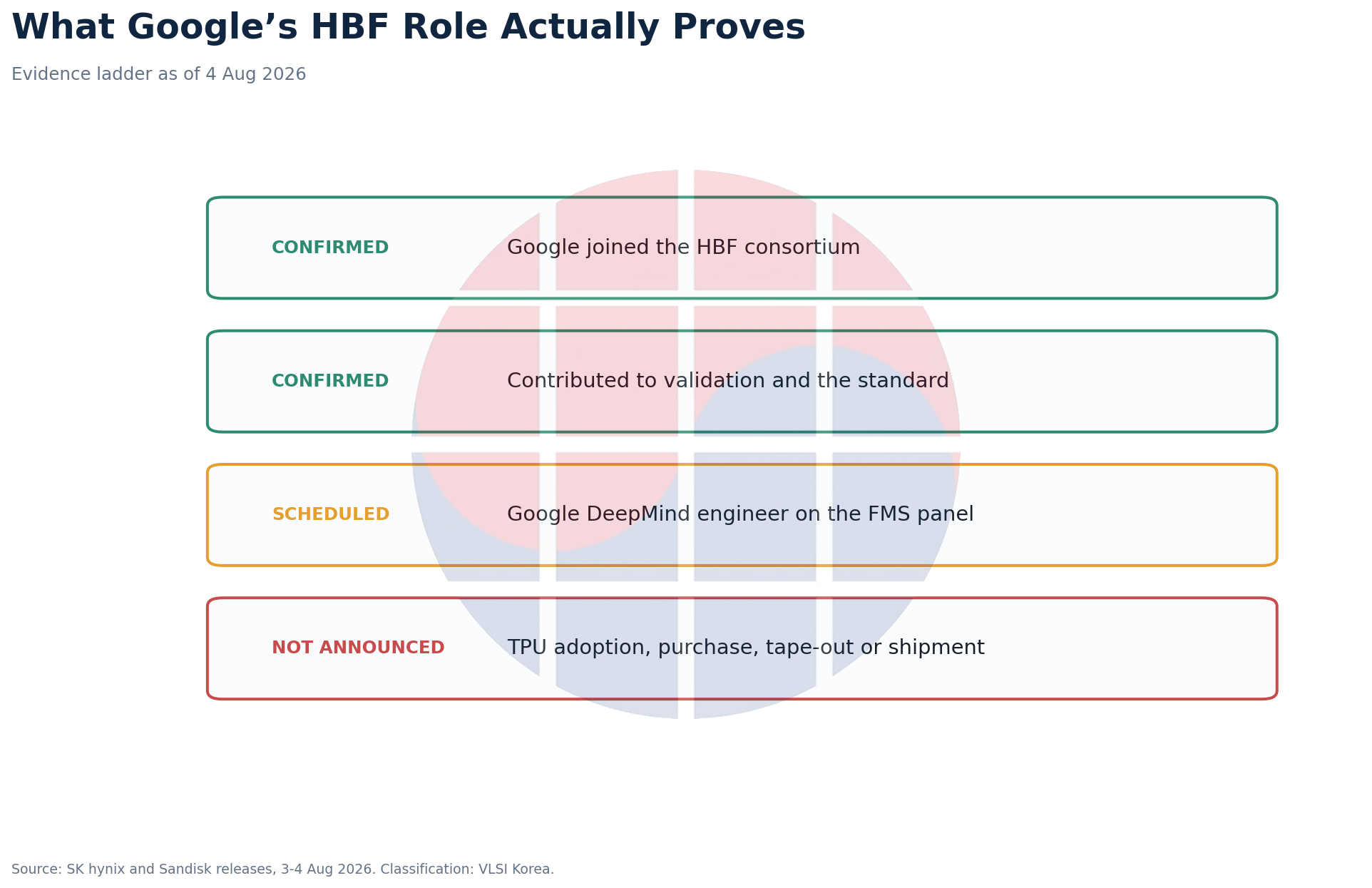
Sandisk and SK hynix said on 3-4 August 2026 that Google and Tenstorrent had joined HBF standardization. They described both companies as significant contributors to technology validation and establishment of the standard.
The releases do not name a TPU generation, a Google Cloud service, a purchase volume, a supplier selection, a tape-out or a sample result. “Google is participating in HBF development” is supported; “Google TPU has adopted HBF” is not.
1. What is confirmed and what remains blank
The SK hynix release and the joint Sandisk-SK hynix announcement establish three points. Google joined the consortium, contributed to validation and standardization, and Google DeepMind Senior Staff Engineer Xiaoyu Ma was scheduled to join an FMS panel on 6 August.
The releases name Google, not a specific Google Cloud or TPU product team. A Google DeepMind engineer can define system requirements without committing any particular accelerator generation to the device.
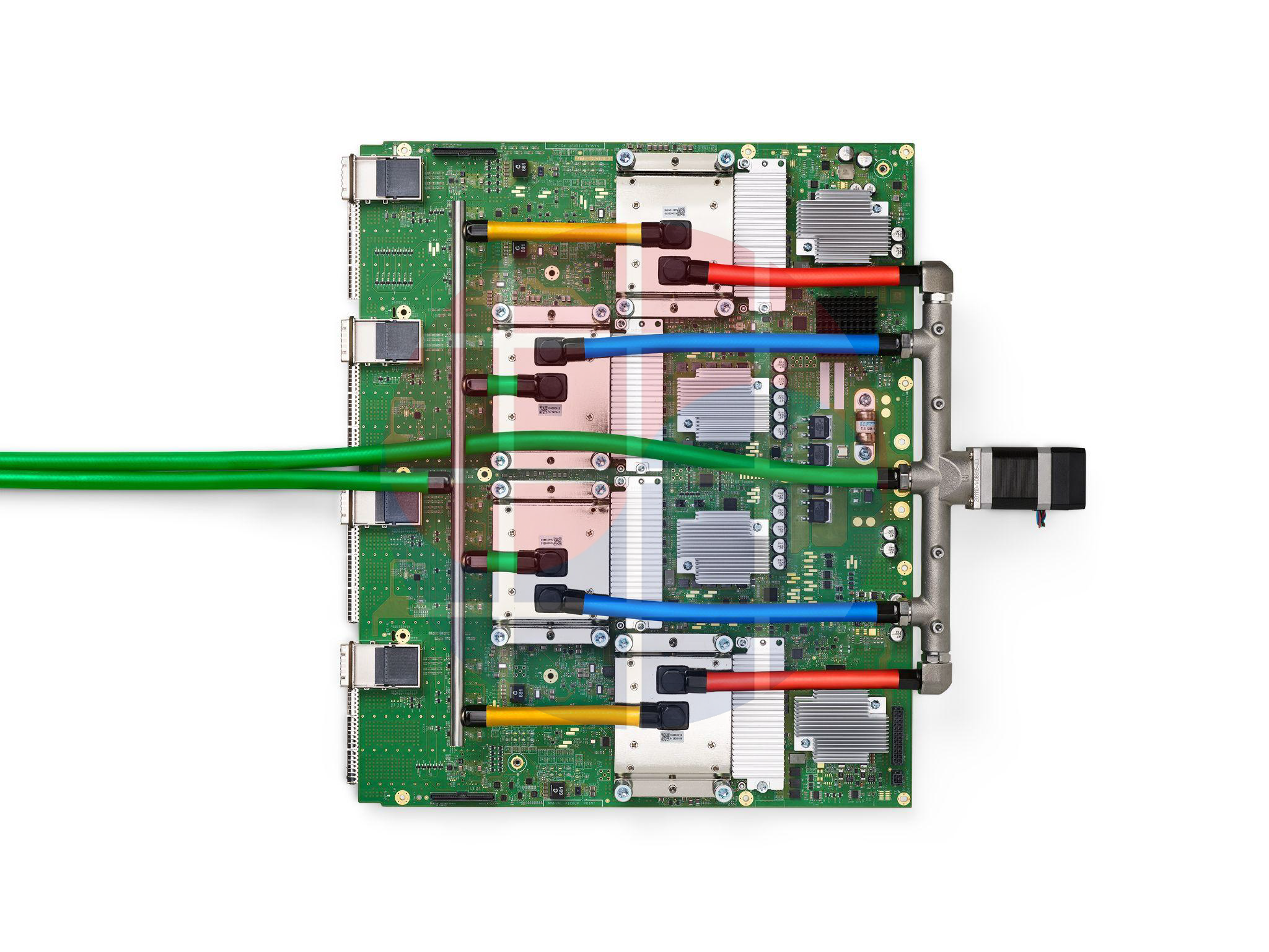
The reusable image above is a TPU v4 board, not an HBF device. It supplies physical context for Google's existing accelerator lineage; its HBM stacks must not be relabelled as HBF.
Individual advice and corporate participation also need separation. Sandisk named Google Distinguished Engineer David Patterson to its HBF Technical Advisory Board in July 2025, while the August 2026 release explicitly says corporate Google joined the standardization consortium. Together they show sustained interest, not a supply contract.
VLSI Korea confirmed that the High Bandwidth Flash Workstream is listed under OCP Storage. We could not independently download the new specification file from the OCP contribution system at publication time, so detailed figures were cross-checked against the two official releases and the Sandisk fact sheet.
2. What the first HBF specification actually covers
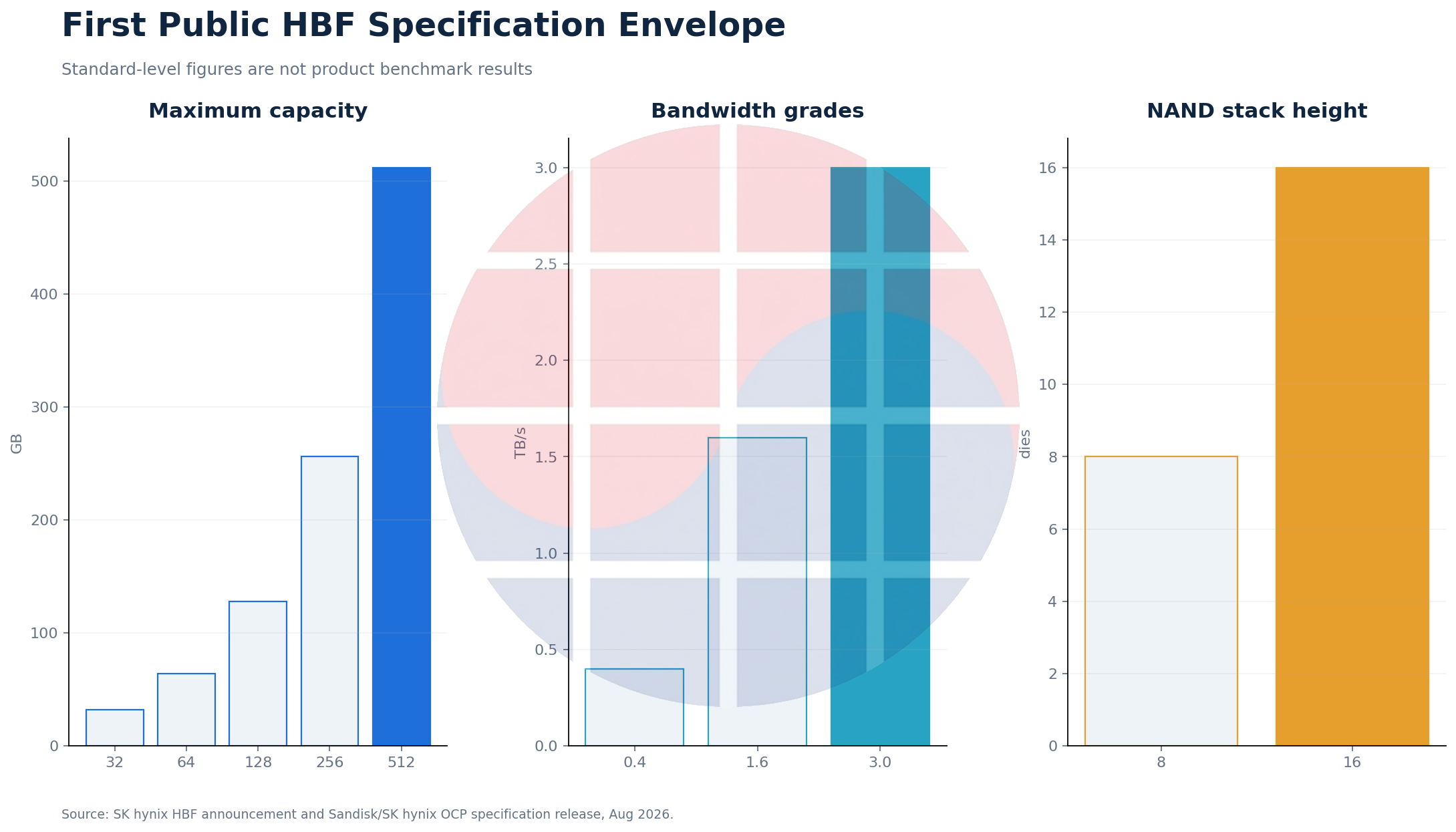
The first public envelope tops out at 512 GB per stack and uses eight or sixteen NAND dies. It defines three bandwidth grades from roughly 0.4 to 3.0 TB/s and adopts UCIe as the host interconnect.
A 512 GB capacity divided across sixteen dies implies 32 GB, or 256 Gb, per die. That arithmetic matches the 256 Gb die in Sandisk's 2025 fact sheet, but it does not reveal usable capacity after spare blocks, ECC and yield management.
The published scope includes the xPU-HBF host interface, basic performance expectations, electrical characteristics, stack reliability, packaging and software read-write guidance. HBF is therefore an attempt to define the boundary among the flash array, controller, package and system software, not merely a die-stacking recipe.
UCIe standardizes physical and protocol layers for package-level die-to-die links. Its selection gives an xPU and an HBF controller a common packaging path, but an existing UCIe controller cannot treat NAND as ordinary memory without substantial flash management.
Flash needs bad-block handling, ECC, read-disturb management, program-erase endurance, garbage collection and address translation. HBF's commercial value depends on where that complexity is hidden and whether the device can deliver predictable accelerator-class latency and bandwidth.
SK hynix separately introduced 375-layer V10 NAND and a claimed 2.5 times power-efficiency improvement in the same event announcement. The company did not say V10 is the production media inside HBF, so describing HBF itself as a 375-layer product would join two unconnected facts.
3. The structural reason Google could care
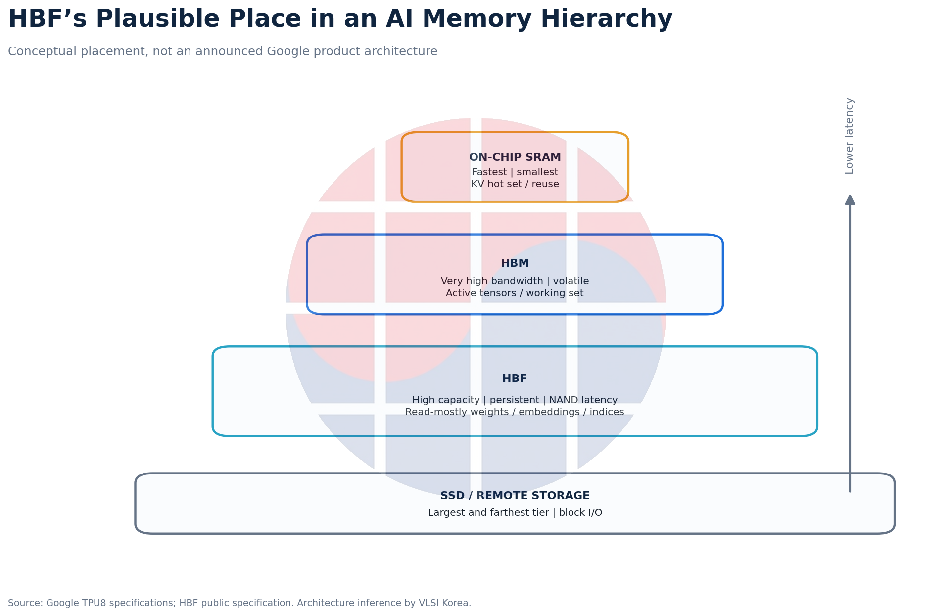
Google's newest disclosed accelerator architecture shows the missing tier more clearly than it shows a replacement target. According to the TPU8 technical deep dive, inference-oriented TPU8i has 288 GB of HBM, 8,601 GB/s of HBM bandwidth and 384 MB of SRAM dedicated to KV-cache acceleration.
Training-oriented TPU8t provides 216 GB of HBM at 6,528 GB/s and uses TPUDirect Storage to reach Lustre. Google already operates a hierarchy of on-chip SRAM, HBM and external storage, assigning data according to reuse and latency.
The 512 GB HBF ceiling is 1.78 times TPU8i's total HBM capacity, while 3.0 TB/s is about 35 percent of TPU8i's whole HBM bandwidth. This is an envelope comparison, not a head-to-head product benchmark: one number is a per-stack HBF ceiling and the other describes an accelerator's complete HBM subsystem.
The plausible role is therefore a new read-oriented tier below HBM rather than the removal of HBM. Active tensors and latency-sensitive state stay in HBM, while weights, embeddings or vector indexes with longer reuse distances move into HBF.
A PACT paper coauthored by Google researchers found that off-chip parameter movement could consume 50.3 percent of inference energy in the edge workloads studied. That percentage cannot be transplanted to a datacenter TPU, but it independently supports the mechanism: placing more model data close to compute can matter as much as adding arithmetic.
Our most likely interpretation is that Google contributes model-serving requirements for page size, prefetching, recovery, tensor placement, performance isolation and observability. The public phrase “technology validation and establishment of the standard” supports that inference, but the consortium has not disclosed Google's specific technical submissions.
4. A 405B-model calculation exposes both the opportunity and limit
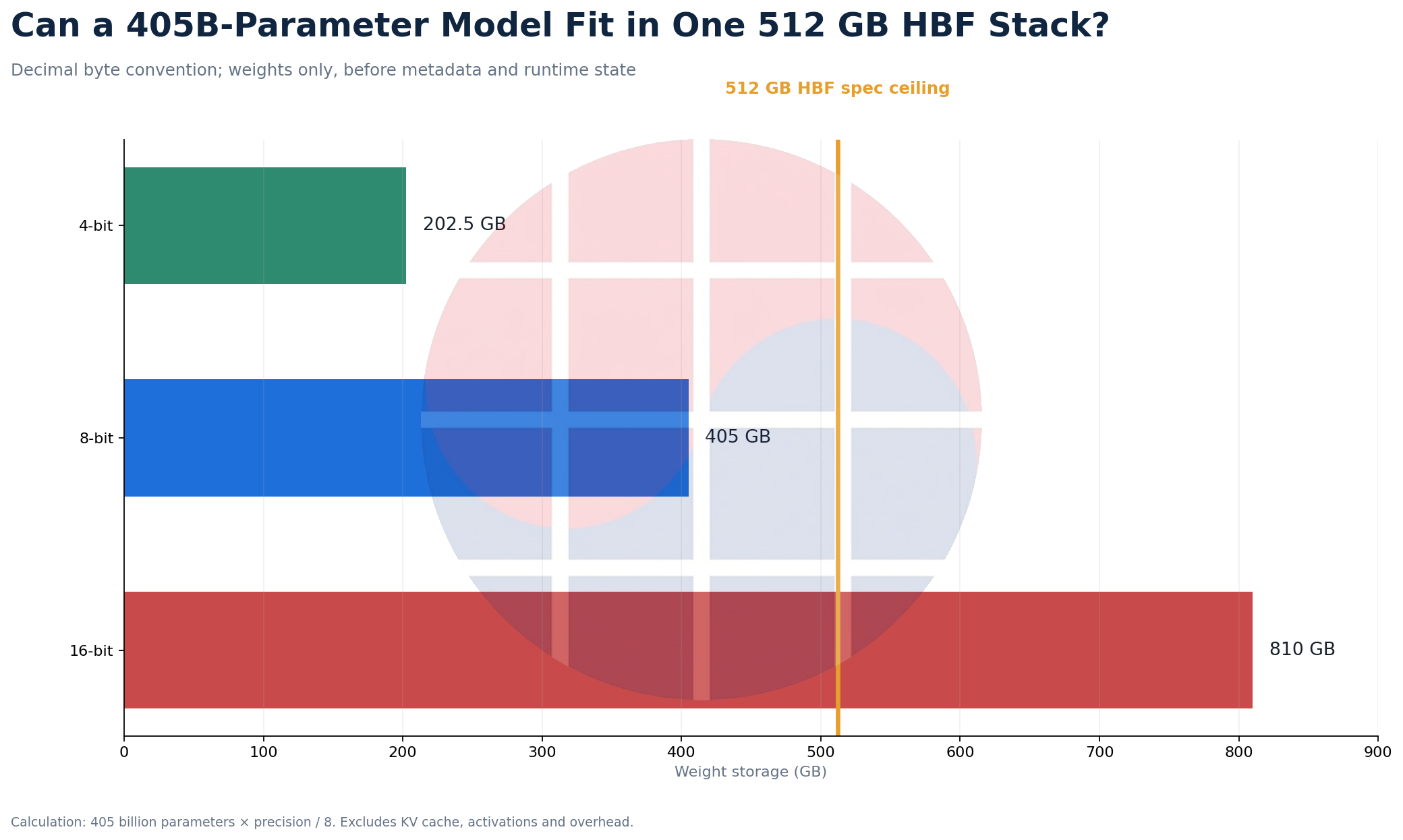
A model with 405 billion parameters occupies about 405 GB when its weights use eight bits. It fits arithmetically within a 512 GB HBF stack with 107 GB left, but that statement excludes KV cache, activations, scales, metadata and reserve capacity.
Sixteen-bit weights require about 810 GB and exceed one stack; four-bit weights require about 202.5 GB. Precision and compression therefore determine system value, and every “the model fits” claim must state the data format and what is excluded.
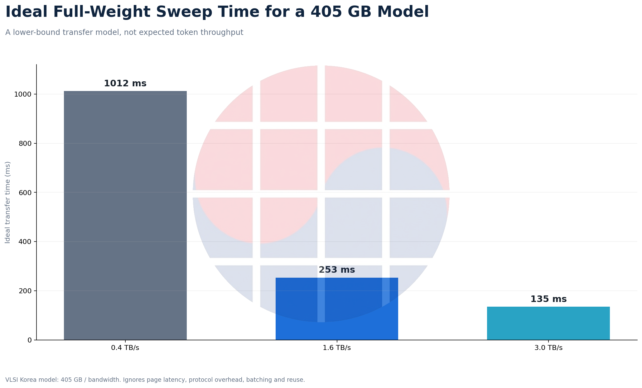
The lower-bound time to sequentially transfer 405 GB is about 1.01 seconds at 0.4 TB/s, 0.253 seconds at 1.6 TB/s and 0.135 seconds at 3.0 TB/s. This is a bandwidth-only floor, not measured token throughput.
Under the deliberately harsh assumption that a dense model rereads every weight for every token, the respective single-stream ceilings are about 0.99, 3.95 and 7.41 token/s. Batching amortizes a weight read across tokens, while Mixture-of-Experts models change the denominator by activating only part of the model.
NAND page latency, small random reads, protocol efficiency, ECC, queuing and thermal throttling push the other way. The decisive measure is not a peak interface number but sustained useful bandwidth and the software's ability to manufacture locality.
Sandisk's 2025 internal simulation reported a 2.2 percent performance gap for Llama 3.1 405B against a hypothetical unlimited-HBM system. It ran one kernel at a time, ignored HBM's capacity disadvantage and modelled HBF rather than measuring production silicon, so it is a vendor simulation rather than a validated benchmark.
5. Workloads that fit HBF and workloads that do not
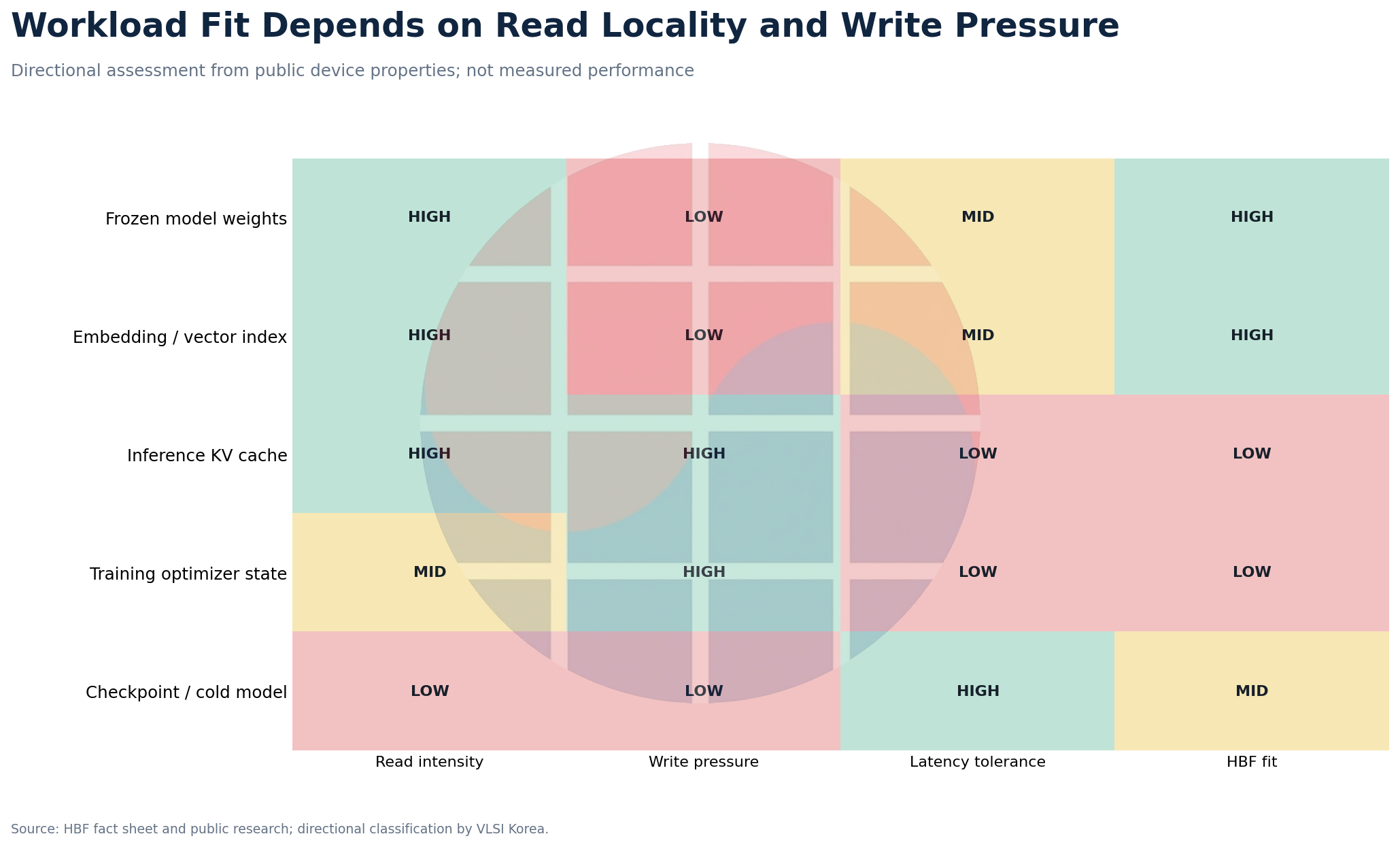
Frozen weights are the strongest initial candidate. Inference servers read them repeatedly and update them rarely; persistence could also reduce the time and energy spent copying a complete model from storage into HBM during deployment.
Embedding tables and vector-search indexes are candidates because they are large and mostly read-oriented. Sandisk's 2025 FMS material and the 2026 HAVEN preprint discuss RAG, recommendations and approximate nearest-neighbor search, but no customer deployment latency has been disclosed.
KV cache is harder. Google emphasizes dedicated SRAM for KV cache in TPU8i because generation continually writes this state and token latency matters; HBF might hold colder sessions but lacks public write-latency and endurance data for the hottest KV tier.
Training optimizer state and checkpoints offer capacity demand but impose much greater write pressure. They should not be treated as leading HBF workloads until endurance, write amplification, consistency and recovery costs are public.
The July 2026 FlashAccel preprint similarly identifies latency, utilization, writes and endurance as system problems alongside capacity. A preprint explores a possibility; it does not validate a supplier's product performance.
6. Five engineering problems decide whether HBF ships at scale
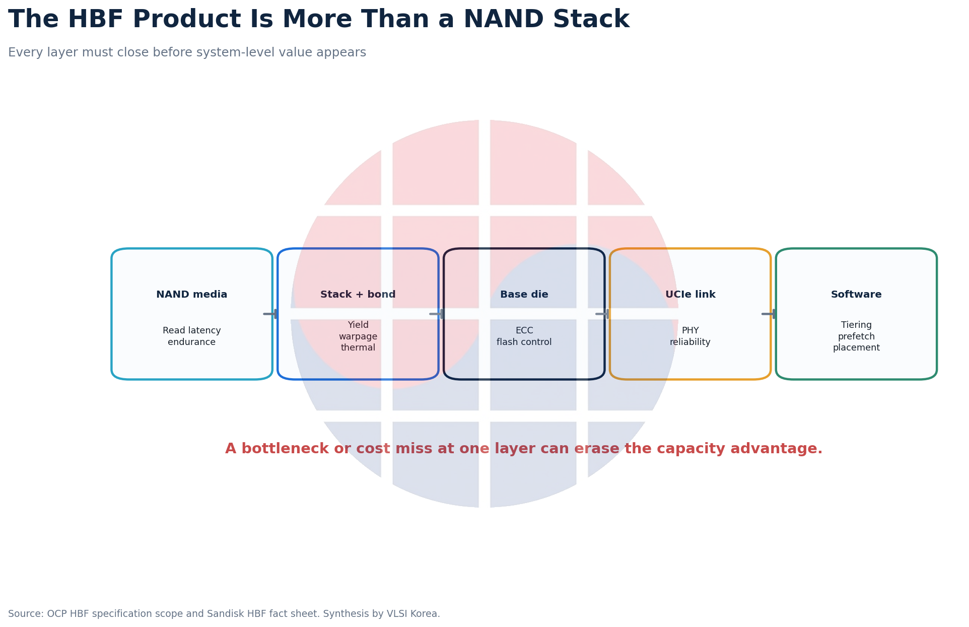
First is NAND read latency and small random access. A 3 TB/s interface cannot create application bandwidth if the arrays lack enough parallelism and queue depth to keep it occupied.
Second is the base die and controller. Unlike an HBM logic base, HBF must translate flash mapping, ECC, bad-block and wear information into an accelerator-friendly address model.
Third is sixteen-die stack yield, warpage and heat. Sandisk presents CMOS directly Bonded to Array, or CBA, as an advantage, but known-good-die supply and bond yield will govern finished-stack economics.
Fourth is power. NAND needs no refresh, yet concurrent array reads, ECC, the UCIe PHY and controller consume energy; nonvolatility alone does not predict stack-level power.
Fifth is software. Compilers and runtimes need reuse distance and access-pattern information to place tensors, prefetch pages and evict data between HBM and HBF.
Operations add another question: what happens when part of a stack degrades? Capacity sparing, package replacement granularity and model-replica movement can materially change total cost.
A credible evaluation therefore needs more than peak read bandwidth. It needs latency distributions by page size, sustained bandwidth, bandwidth per watt, write endurance, retention, bad-die tolerance, sixteen-high yield and measured software overhead.
7. Google, Sandisk, SK hynix and the Korean supply-chain angle
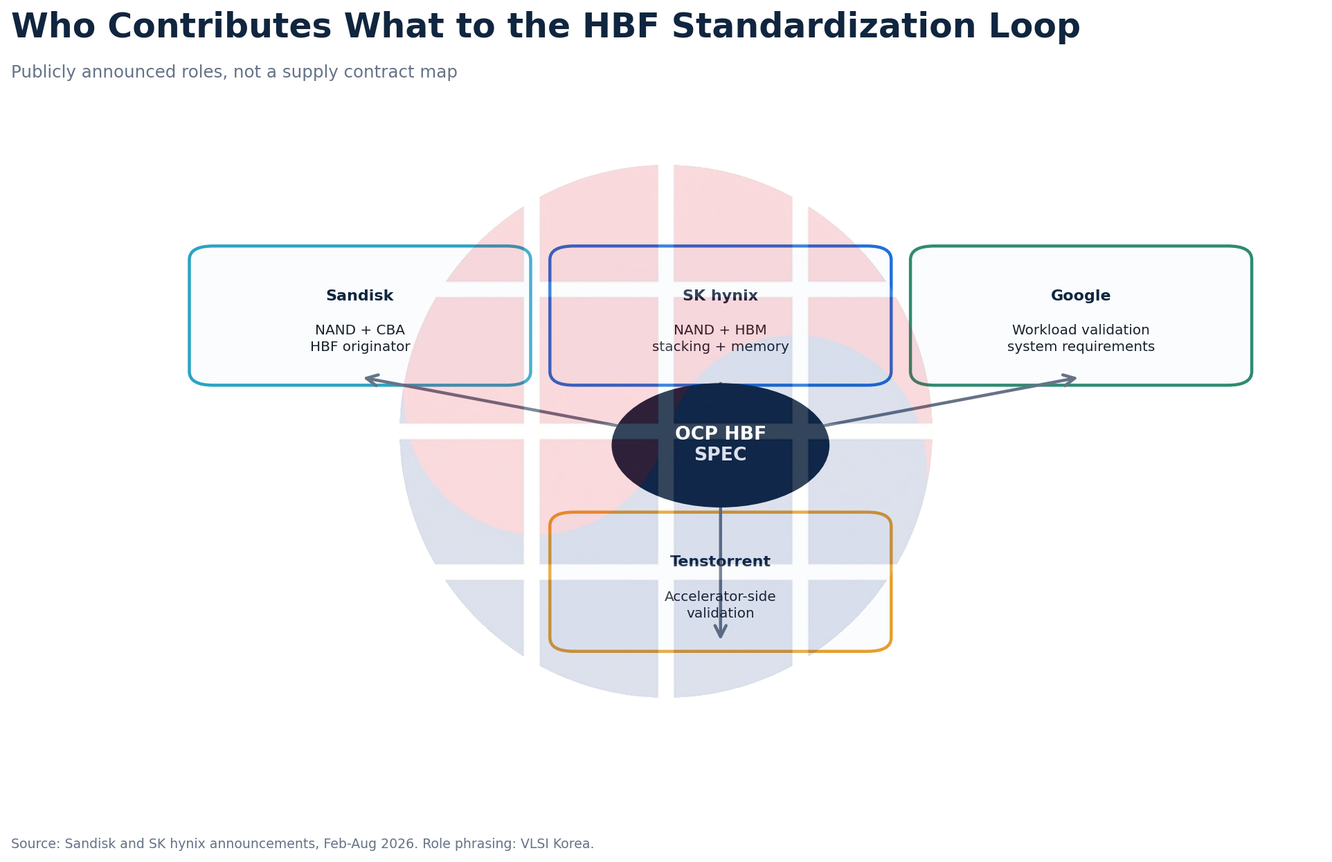
Sandisk contributes the HBF concept, CBA-based NAND technology and a product roadmap. SK hynix contributes NAND, HBM, high-stack packaging and a memory supplier's standardization capability.
Google and Tenstorrent bring accelerator and system-validation perspectives. Their presence can prevent a memory-vendor specification from optimizing only peak device numbers while neglecting error models, software interfaces and real workload behavior.
For Korea, the opportunity is not the simplistic claim that HBF follows or replaces HBM. If HBM holds the hottest data, HBF holds large read-mostly assets and enterprise SSDs hold colder data, SK hynix can connect three memory tiers into one system proposal.
The value pool cannot be estimated from NAND wafer volume alone. Early HBF may have modest unit volume but high package value because it includes a base die, controller, stacking, test, UCIe IP and firmware.
The counterweight is economics. Poor sixteen-high yield or an expensive controller could make expanded HBM, LPDDR tiers, CXL memory or accelerator-attached SSDs cheaper; HBF must save more accelerators, power and rack space than its premium package costs.
As of 4 August 2026, VLSI Korea found no official announcement that Samsung Electronics, Micron or Kioxia had joined this HBF consortium. Absence of an announcement is not proof of absence, and the Sandisk-Kioxia NAND manufacturing joint venture does not automatically make Kioxia an HBF standard participant.
The first OCP technical specification is also a starting point. It does not yet demonstrate a mature multi-vendor interoperability and certification ecosystem comparable to an established shipping memory standard.
8. Roadmap, three scenarios and conditions that break the thesis
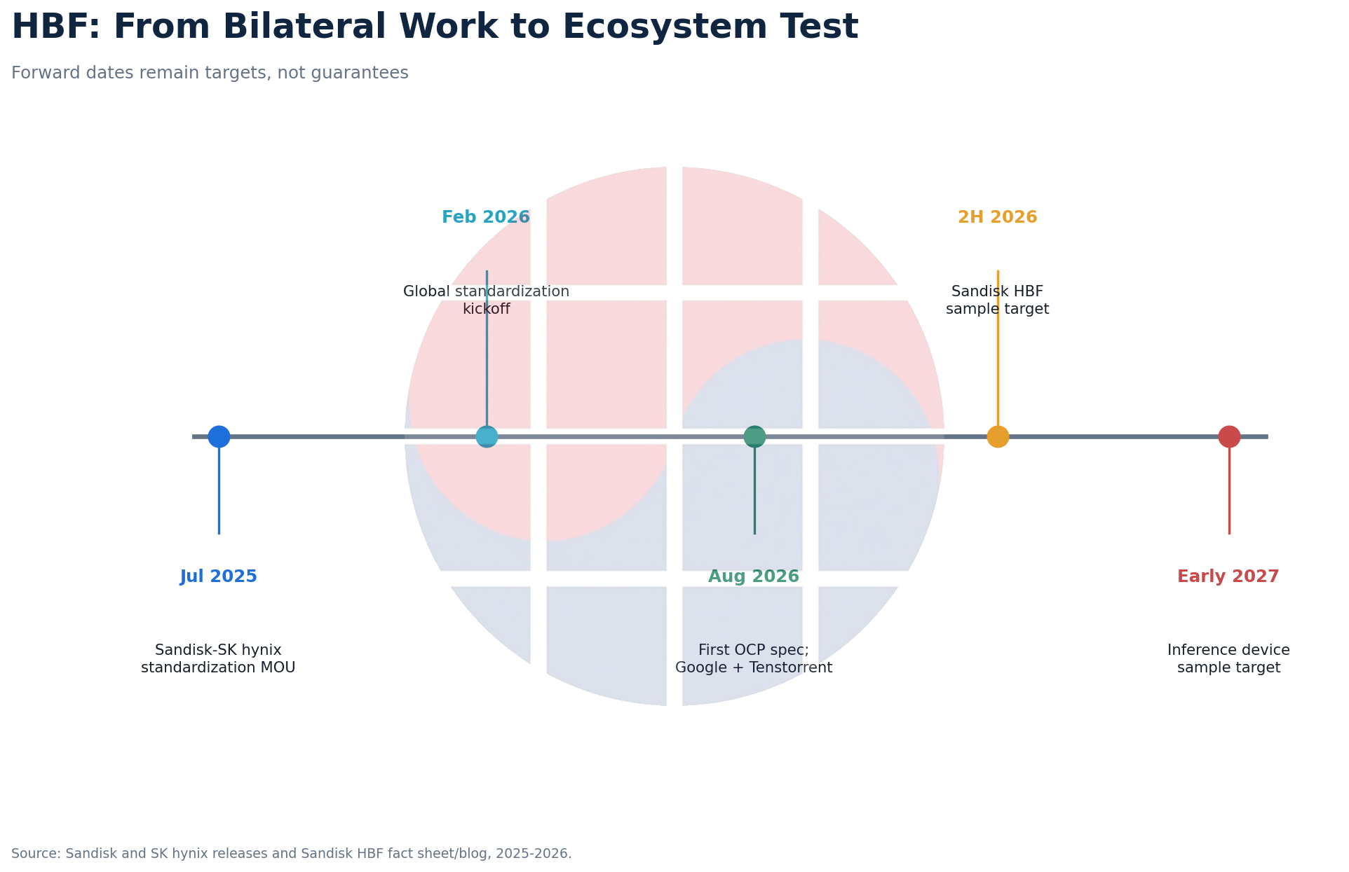
Our base case is that limited partners receive HBF memory samples in the second half of 2026 and inference-device samples in early 2027, with validation beginning on read-mostly weights and embeddings. Google's participation improves system relevance but does not guarantee a named Google customer product.
The upside case requires real silicon to sustain at least the first-generation bandwidth target with acceptable latency, allowing a 512 GB tier to reduce the accelerator count otherwise forced by HBM capacity. HBF would then complement HBM while increasing memory content per AI server.
The downside case is a sample delay combined with weak small-read latency, insufficient endurance, poor sixteen-die yield or excessive data-movement software. If customers solve the same problem more cheaply with larger HBM, LPDDR, CXL or direct storage, HBF remains a niche.
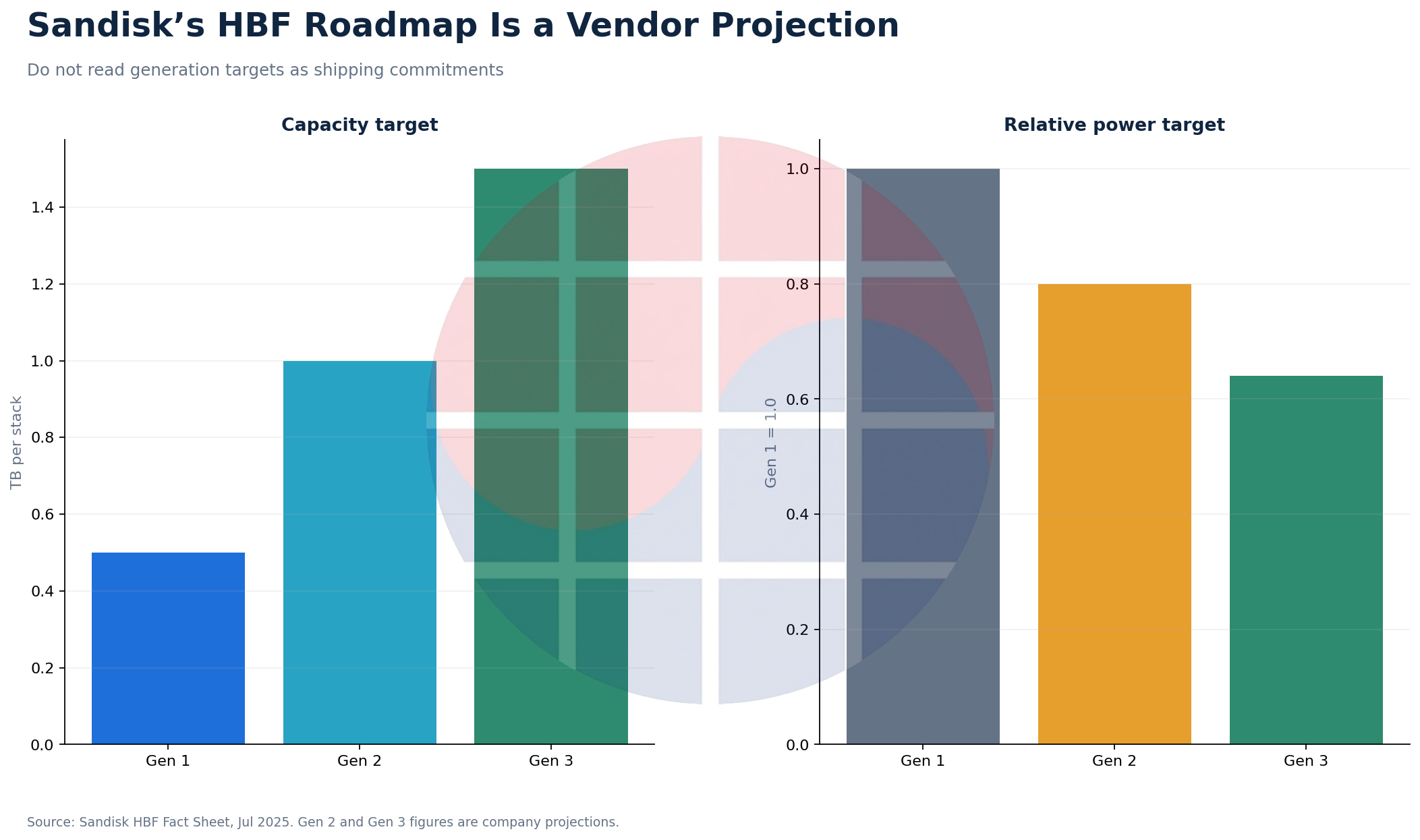
Sandisk's 2025 roadmap lists 512 GB and 1.6 TB/s for generation one, more than 2 TB/s and 1 TB for generation two, and 3.2 TB/s and 1.5 TB for generation three. Relative power targets are 1.0, 0.8 and 0.64; later figures are company projections and should not be confused with the 3.0 TB/s grade in the 2026 OCP envelope.
The first thesis breaker is measured silicon whose latency, sustained bandwidth and endurance fail to lower total cost against an HBM-plus-SSD hierarchy for read-oriented inference. The second is a UCIe-package and sixteen-high yield penalty that eliminates HBF's cost-per-capacity advantage.
Next observations are Google's architecture requirements at the scheduled 6 August FMS panel, whether Sandisk meets its second-half 2026 sample target, and the named customers and benchmarks for early-2027 inference-device samples. Read-latency distributions, useful bandwidth, power, endurance and required software changes need numbers.
The present conclusion is narrow but important. Google joining turns HBF from a memory-vendor proposal into a standard tested with an accelerator consumer, but it does not yet turn HBF into a confirmed TPU component.
Sources
- SK hynix, First Open HBF Standard and FMS 2026 participation, 4 Aug 2026
- Sandisk and SK hynix, first OCP HBF technical specification, 3 Aug 2026
- Open Compute Project, High Bandwidth Flash Workstream listing
- Sandisk HBF Fact Sheet, Jul 2025
- Sandisk, Memory-Centric AI, 11 Aug 2025
- Sandisk HBF Technical Advisory Board, 24 Jul 2025
- Sandisk and SK hynix HBF standardization MOU, 5 Aug 2025
- Sandisk and SK hynix global standardization kickoff, 25 Feb 2026
- Google Cloud, TPU8t and TPU8i technical deep dive, 22 Apr 2026
- UCIe Consortium, specifications
- Ma et al., PACT, arXiv:2109.14320
- FlashAccel preprint, arXiv:2607.10186
- HAVEN preprint, arXiv:2603.01175
- Wikimedia Commons, TPU v4 image, CC BY 4.0
Methodology. We compared the company releases available on 4 August 2026, the OCP workstream listing, Google TPU documentation, the UCIe specification page, papers and the original page for the reusable image. Supplier performance and roadmap figures are labelled as claims or targets, while VLSI Korea calculations expose inputs and exclusions.
AI-assistance note. AI tools assisted source classification, arithmetic checks, chart production and the translation draft; an editor rechecked source links and material figures. The feature is an AI-generated concept image and does not depict a real product.
This article is provided for informational purposes only and does not constitute a recommendation to buy or sell any security. Figures and factual statements are based on publicly available sources, including company filings, news reports, and market research, and may contain errors in the source material or in the preparation of this article. The author may own shares in companies mentioned. All investment decisions and their outcomes are the reader's responsibility.
Related reading