VLSI Korea
A 256-Core Server CPU Is a Memory-I/O Problem: The Diamond Rapids Throughput Envelope
A 256-core server CPU scales only where the memory, I/O, coherency, and package envelopes close together.


🆓 Free article · Anyone can read this article for free
The answer is that a 256-core server CPU is constrained less by the headline core count than by the point where usable memory bandwidth, on-package movement, coherent expansion, and board I/O all close at once. At Hot Chips 2026 on August 24, Intel disclosed up to 256 cores, 1.28 GB of last-level cache, sixteen memory channels at 12,800 MT/s, 128 PCIe 6.0 lanes, and CXL 3.0 for Diamond Rapids. That envelope shows an attempt to widen the bottlenecks around a large CPU. Peak specifications, however, do not prove sustained workload throughput, latency, utilization, or rack economics.
This article serves two reader jobs. Server architects and performance engineers can decompose a core-count claim into four envelopes: memory, I/O, coherency, and package. Procurement, product, and infrastructure owners can ask whether useful work per watt, rack, and software license improves rather than comparing sockets by cores alone. It improves two decisions: which workloads belong on a 256-core socket, and whether the next dollar should go to CXL memory, accelerators, storage, networking, or software locality.
1. What Intel disclosed, and what remains undisclosed
Intel's August 24 announcement positions Diamond Rapids as a compute foundation for enterprise-scale agentic AI. The disclosed maxima are 256 cores, 1.28 GB of LLC, sixteen memory channels at 12,800 MT/s, and 128 PCIe Gen6 lanes with CXL 3.0. Intel also names 18A-P, Foveros Direct 3D, UCIe-S, a unified memory fabric, APX, and enhanced AMX. The official Hot Chips program independently confirms the presentation identity and its August 24 CPU-session placement.
The missing data are equally important. The public page does not provide a complete product table covering SKU-level core counts, memory population, TDP, sustained bandwidth, NUMA topology, UCIe lane allocation, cache-slice access cost, latency by CXL-device configuration, and workload benchmarks. A maximum is not necessarily a guaranteed point at which every other maximum is available simultaneously. “Up to” should not be read as a promise that all disclosed limits close on one operating configuration.
Dividing 1.28 GB by 256 yields an arithmetic average of 5 MB per core, but that is not a private allocation. Shared-cache value depends on addressing, slices, fabric topology, contention, and locality. Likewise, 128 PCIe lanes do not imply that every lane continuously moves useful payload. Link widths, switching, protocol overhead, traffic direction, device behavior, and host-memory pressure determine the realized result.
The consensus is that Intel is scaling cores, memory, packaging, and I/O together. The narrower VLSI Korea view is this: 256 cores are a balance sheet, not a performance result. If the workload cannot use the sixteen channels, UCIe-S, PCIe 6.0, and CXL 3.0 as one balanced system, additional cores may add queueing or idle capacity. The disagreement is between “more cores imply proportionally more throughput” and “proportional scaling appears only where all four envelopes overlap.”
2. The first envelope: interpreting 1.638 TB/s across sixteen channels
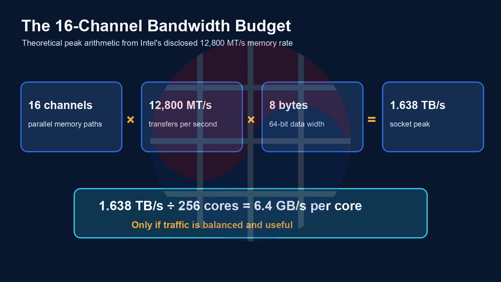
Assuming a 64-bit payload channel, the theoretical peak is sixteen multiplied by 12.8 billion transfers per second multiplied by eight bytes, or 1.6384 TB/s. Dividing that evenly among 256 cores gives 6.4 GB/s per core. This is not a Diamond Rapids measurement. It combines Intel's disclosed transfer rate with a standard 64-bit payload width. ECC traffic, commands, refresh, bank conflicts, controller efficiency, read/write mix, NUMA locality, and software access patterns can all reduce sustained payload bandwidth.
Whether 6.4 GB/s per core is sufficient depends on the workload. Code with high cache reuse and arithmetic intensity uses the external memory interface less aggressively. Pointer chasing, graph analytics, in-memory scans, and memory-bound scientific kernels can consume latency and bandwidth quickly. Under dense virtualization, independent tenants can share channels and LLC capacity while amplifying tail latency. A procurement benchmark should therefore report socket bandwidth, per-core bandwidth, local and remote latency, and a tail percentile instead of only an aggregate score.
The common error is to substitute peak bandwidth for application bandwidth. A rate of 12,800 MT/s is a transfer rate, and 1.638 TB/s assumes every channel is populated and efficiently filled. Real platforms have DIMM population rules, ranks, timing limits, controller scheduling, and page locality. A configuration optimized for capacity may not be the one that maximizes bandwidth. “Supports sixteen channels” and “sustains the top rate across sixteen channels in the deployed SKU” are different claims.
The operating decision is to read core and memory-controller utilization together. High core idle time with saturated memory controllers argues for data placement, compression, cache blocking, partitioning, or fewer active cores before another core-count upgrade. Available memory headroom with saturated cores suggests compute, vectorization, accelerator offload, or dependency limits instead. A bottleneck is the place where a queue accumulates, not the name of a component.
3. The second and third envelopes: UCIe, PCIe, and CXL are different contracts
The UCIe Consortium defines UCIe as a package-level die-to-die standard spanning the physical layer, protocol stack, software model, and compliance testing. UCIe 2.0 expanded manageability, testability, debug, and 3D packaging. UCIe 3.0 added 48 and 64 GT/s rates, a longer sideband channel, fast throttle, emergency shutdown, and runtime recalibration. Intel's UCIe-S disclosure signals modular die construction, but the public announcement does not expose the number of links, topology, retry behavior, repair policy, or thermal guardband.
PCI-SIG describes PCIe 6.0 as a 64 GT/s raw-rate interface providing up to 256 GB/s of aggregate bidirectional bandwidth for x16. PAM4, FLIT mode, lightweight forward-error correction, and CRC are core features. Diamond Rapids' 128 lanes can connect many accelerators, NICs, and storage devices in principle. The useful result still depends on device demand, switch oversubscription, DMA patterns, traffic direction, and competing host-memory traffic.
The CXL Consortium's public 3.0 release emphasizes 64 GT/s, memory sharing and pooling, enhanced coherency, peer-to-peer communication, and multi-level switching. CXL can expand capacity and composability, but remote capacity is not guaranteed to match local-memory latency or bandwidth. Poor page placement, hot/cold tiering, operating-system policy, or device-controller behavior can increase capacity with little improvement in elapsed workload time.
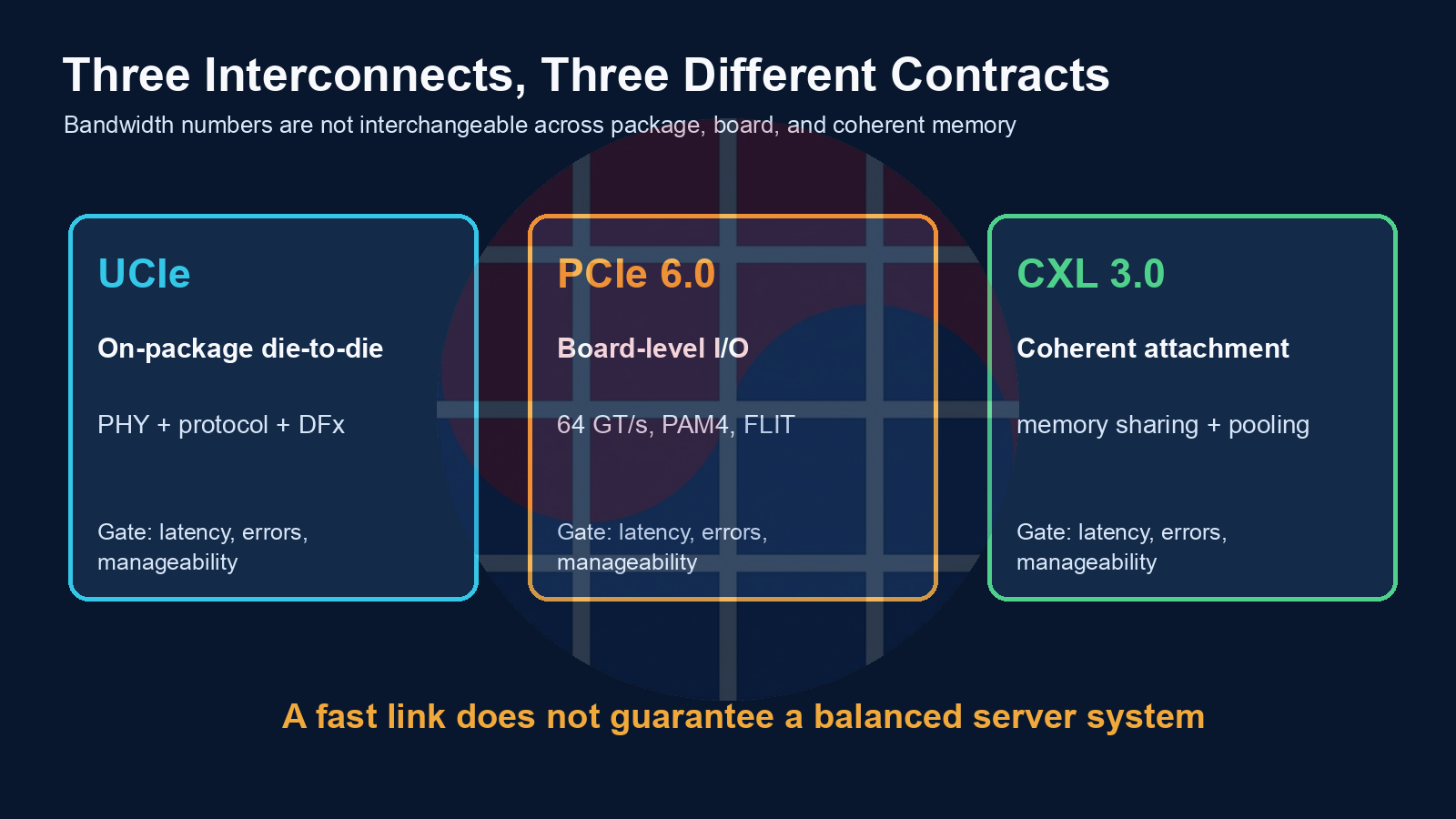
Adding the three interface rates into one “system bandwidth” number is invalid. UCIe controls movement and management inside the package; PCIe transports board-level I/O; CXL adds coherent protocols and memory semantics. A byte may cross only one boundary or traverse several. A useful performance model treats each path's latency, concurrency, retry, coherency traffic, and data reuse separately.
4. The fourth envelope: packaging changes latency, repair, and yield
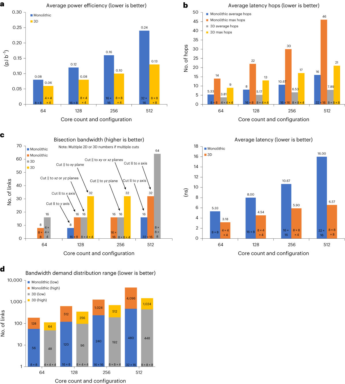
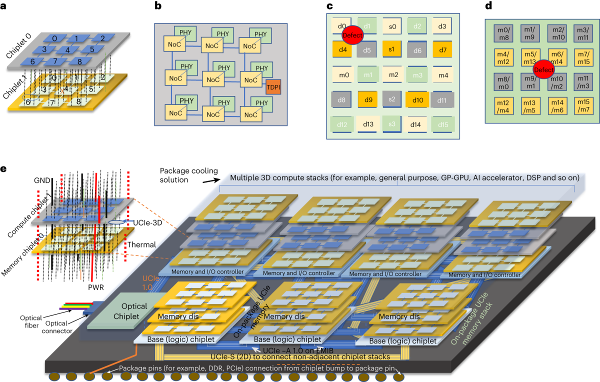
The open-access UCIe-3D paper proposes that, as bump pitch shrinks, short-distance links can achieve high bandwidth density and low power at lower operating frequency. Figure 2 shows NoCs, PHYs, repair subclusters, stacked compute, and memory/I/O. Figure 6 models hops, latency, bisection bandwidth, and power for monolithic and 3D networks. The authors include a 256-core scenario, but those results must not be transferred to Diamond Rapids. Their relevance is mechanistic: as core count grows, topology and hop distribution become first-order workload variables.
A package is not a passive wiring board. Core tiles, memory and I/O tiles, cache, power delivery, thermal paths, test access, and known-good-die strategy are coupled. Splitting a die can improve reticle flexibility and yield management. It also introduces die-to-die latency, PHY area, protocol overhead, assembly yield, thermal coupling, and failure-isolation costs. The labels 18A-P and Foveros Direct 3D alone do not quantify the net outcome.
Intel's public 18A page presents RibbonFET, PowerVia, and company-claimed performance, power, and density improvements. Those comparisons are platform claims against Intel 3 under stated conditions, not full-system Diamond Rapids benchmarks. A CPU buyer needs a chain from process metrics to socket power, frequency distribution, sustained memory throughput, package loss, yield, and availability.
Failure economics also change at the package boundary. If one tile's defect can be absorbed through binning or repair, modularity can improve economics. If a stack or bond failure removes the entire package, the benefit of known-good dies narrows. Field telemetry matters as well: can a degraded link reduce width and continue operating, or does it fail the socket? UCIe's manageability and test features matter because they affect both manufacturing yield and field serviceability.
5. The Four-Envelope Throughput Test
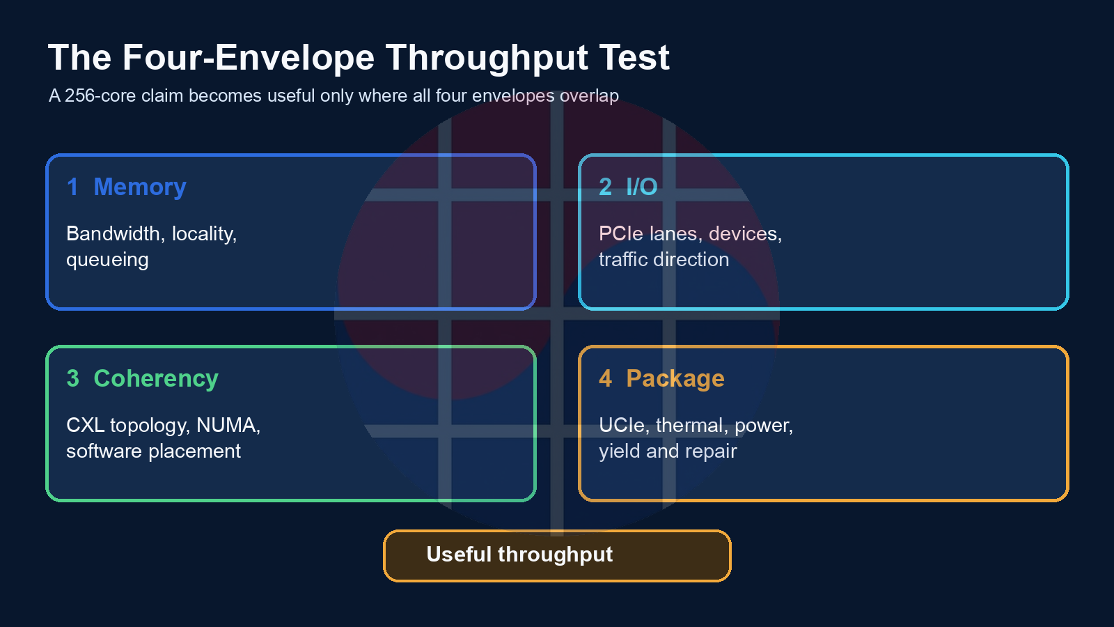
This article proposes the Four-Envelope Throughput Test, which uses the narrowest envelope as the first approximation of system throughput. It is a decision framework, not an exact product model. The memory envelope covers sustained bandwidth, locality, and queueing. The I/O envelope covers lanes, attached devices, traffic direction, and switching. The coherency envelope covers CXL topology, NUMA behavior, page placement, and software policy. The package envelope covers UCIe topology, thermal limits, power delivery, yield, and repair.
Start by expressing the workload in bytes, operations, working-set size, and a tail-latency target. Labels such as “AI workload” or “database” are too broad. Even token serving divides into orchestration, preprocessing, networking, and key-value-cache movement. EDA compilation, graph traversal, simulation, and place-and-route have different memory behavior. The same 256-core socket can be an excellent fit for one phase and an expensive queue for another.
Next, construct a roofline from measured local-memory bandwidth, not the public peak. Subtract host traffic consumed by accelerators, NICs, and storage. If CXL memory is present, model local and remote tiers separately, including hit ratio and migration cost. Then check whether thermal or power limits lower sustained frequency. The objective is to reveal which queue moves when the system changes.
The decision threshold is not “how much faster is a 256-core CPU?” It is “how much more accepted work completes inside the current rack constraint?” A software license priced by core can erase a hardware throughput gain. An already saturated network or storage tier can turn a CPU upgrade into queue migration. Conversely, socket consolidation may reduce server count, memory duplication, network ports, and operational complexity even when per-core performance does not scale perfectly.
6. Roofline arithmetic: workload intensity sets the value of cores
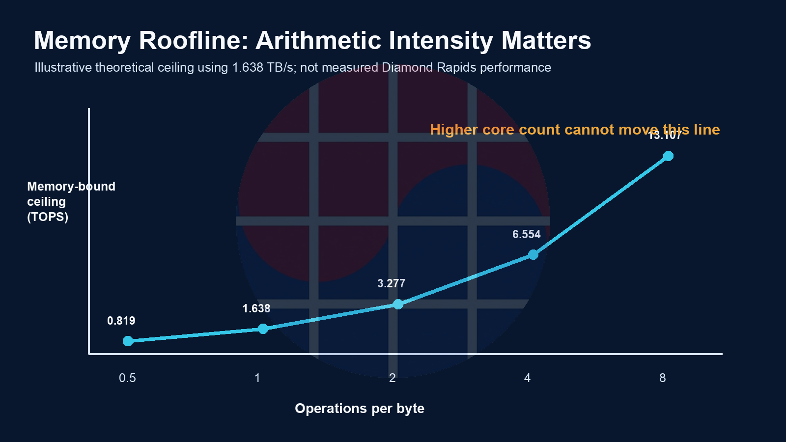
A memory-bound ceiling can be expressed as bandwidth multiplied by arithmetic intensity. Using 1.638 TB/s, the explanatory limits are 0.819 TOPS at 0.5 operation per byte, 1.638 TOPS at 1, 3.277 TOPS at 2, 6.554 TOPS at 4, and 13.107 TOPS at 8. This simplified ceiling ignores instruction mix, vector width, cache reuse, and latency. The lower of that line and the compute peak forms the roofline, indicating the first-order constraint.
The direction matters more than false precision. A low-intensity workload cannot cross the memory line by adding cores. Cache blocking, data layout, compression, prefetch, and locality come first. A high-intensity workload with strong reuse moves away from the memory ceiling, making vector units, frequency, instruction dependencies, and scheduling more important.
The strongest counterargument is that production workloads do not fit on a one-line roofline. That is correct. They have phases, synchronization, network waits, and nonuniform access. The chart is therefore a test-design tool, not a product forecast. Measure bytes per operation and counters by workload phase, identify the memory-bound phase, and intervene only there.
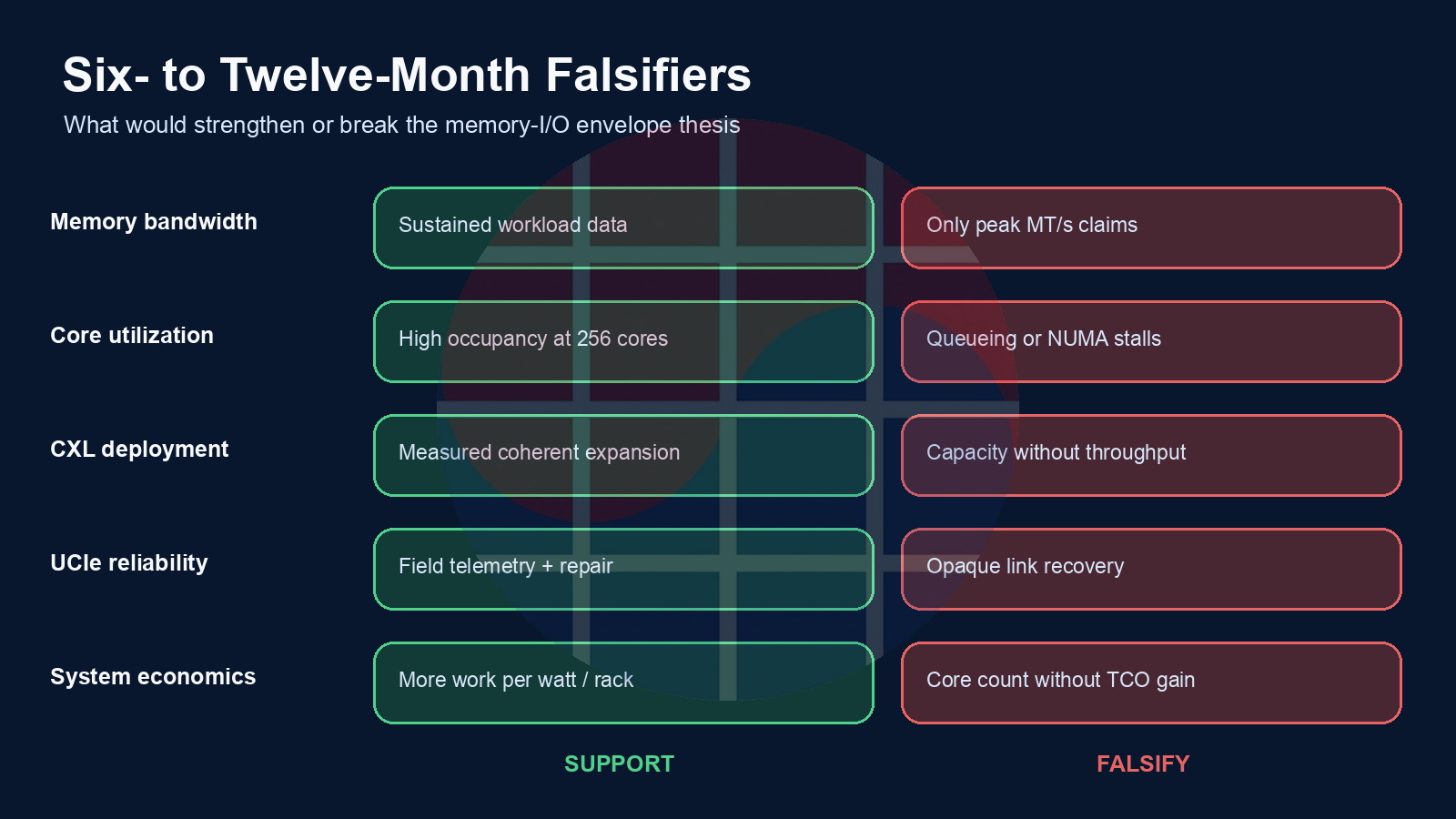
The thesis has clear falsifiers. If public benchmarks reproduce high occupancy at 256 cores across broad workloads while memory, UCIe, and CXL paths retain low tail latency, and if energy and license cost improve per socket or rack, the core-count headline is a good proxy for utility. If only peak channel rates appear while sustained data, NUMA behavior, CXL placement, and field repair remain undisclosed, the specification is still ahead of the evidence.
7. Korea Lens: the data memory, packaging, and system teams should demand
For Korean memory suppliers, a sixteen-channel server is not simply a larger DIMM count. MRDIMM speed bins, signal integrity, thermal margin, controller training, capacity mix, reliability, availability, serviceability, and workload qualification move together. Sustaining 12,800 MT/s requires modules and platforms to close at the same operating point. SK hynix and Samsung Electronics should care more about qualified configurations, sustained bandwidth, correction behavior, throttling, and customer-workload coverage than about the channel announcement alone.
Packaging and substrate teams should not treat UCIe-S as only a protocol name. Bump pitch, routing, power integrity, thermal gradients, test access, repair policy, and assembly yield determine system economics. EDA and verification teams need to add multi-die latency, traffic hotspots, fault injection, firmware bring-up, and telemetry to the sign-off flow. VLSI Korea's recent references on in-network compute and digital-twin release gates point to the same pattern: every new interface increases the importance of ownership and validation contracts.
Server buyers and cloud operators should change the evaluation matrix. In addition to cores, list price, and benchmark scores, include memory bandwidth per core, local and remote latency, CXL-tier hit ratio, PCIe-device saturation, throughput after power capping, and software-license cost per accepted job. Where possible, compare one-socket consolidation against two-socket NUMA on the same workload cost. Migration, tuning, and qualification time may exceed the hardware-price difference.
Universities can use a 256-core system as more than a parallel-programming demonstration. A useful lab measures memory traffic, topology, coherency, and power together. It reports tail latency and imbalance rather than only average throughput, and requires students to revise the hypothesis when counters reject the headline. Occupying many cores and filling them with useful work are not the same outcome.
8. Six-to-twelve-month watchpoints and practitioner checklist
By September 30, 2026: watch for a Hot Chips deck or follow-up disclosure covering tile topology, memory fabric, cache, UCIe-S organization, and measured benchmarks. If the evidence remains a peak table, uncertainty remains open.
By December 31, 2026: look for platform, memory, firmware, and CXL-device compatibility documentation. The key question is which DIMM population and operating conditions support sixteen channels at 12,800 MT/s, and with what thermal and power guardbands.
By March 31, 2027: watch for sustained memory bandwidth, local and remote latency, and workload utilization from independent labs or customers. Separate synthetic peaks from application results.
By June 30, 2027: test whether socket consolidation, CXL memory tiering, and accelerator attachment improve work per watt and work per rack. Shipment volume or a launch date alone does not validate the architecture thesis.
The practitioner checklist fits in six questions. Have you measured workload bytes per operation? Have you separated local from remote memory? Have you checked PCIe traffic direction and switch oversubscription? Have you avoided treating CXL capacity as equivalent to local bandwidth? Have you reviewed UCIe and package repair telemetry? Finally, are you comparing accepted work per cost rather than cores?
Record two thesis breakers. First, if independent production benchmarks reproduce near-linear scaling at 256 cores while retaining memory and I/O headroom, this article overstates the bottleneck risk. Second, if UCIe and CXL manageability, repair, and software placement become nearly automatic with negligible operating overhead, the cost of a four-envelope review falls.
The conclusion is simple. Two hundred fifty-six cores are a stress test, not the objective. They reveal the narrowest point across memory, I/O, coherency, and package. Where all four envelopes close, Diamond Rapids' disclosed architecture can create high system value. Where one remains open, additional cores can become a queueing liability rather than a performance asset.
Sources and method
- Intel, Hot Chips 2026 architecture announcement, August 24, 2026. Product numbers are company-reported maxima.
- Intel 18A technology page. Process comparisons are Intel claims, not Diamond Rapids system benchmarks.
- Hot Chips 2026 official program, used to cross-check the event and presentation identity.
- UCIe Consortium specification index, current when opened August 25, 2026.
- PCI-SIG, PCI Express 6.0 specification resources.
- CXL Consortium, public CXL 3.0 release.
- Das Sharma et al., UCIe-3D system-in-package research, Nature Electronics 7, 244–254 (2024), CC BY 4.0.
- Tom's Hardware and StorageReview, independent disclosure cross-checks, August 24, 2026.
AI assistance note: AI tools supported public-source discovery, arithmetic verification, bilingual consistency checks, visual drafting, and copy editing. VLSI Korea editorial review remains responsible for the thesis, source interpretation, uncertainty labels, and publication decision. The bandwidth and roofline charts are transparent theoretical calculations, not measured Diamond Rapids performance.
This article is provided for informational purposes only and does not constitute a recommendation to buy or sell any security. Figures and factual statements are based on publicly available sources, including company filings, news reports, and market research, and may contain errors in the source material or in the preparation of this article. The author may own shares in companies mentioned. All investment decisions and their outcomes are the reader's responsibility.
Frequently Asked Questions
What did Intel disclose for Diamond Rapids?
Intel disclosed up to 256 cores, 1.28 GB of last-level cache, sixteen memory channels at 12,800 MT/s, and 128 PCIe Gen6 lanes with CXL 3.0. The disclosure was made at Hot Chips 2026 on August 24.
What is Diamond Rapids' theoretical peak memory bandwidth?
Sixteen channels times 12,800 MT/s times eight payload bytes gives 1.6384 TB/s, or 6.4 GB/s per core when divided evenly. This is a theoretical peak, not an observed benchmark.
How much cache is that per core on average?
Dividing 1.28 GB by 256 gives an arithmetic average of 5 MB per core. It is not a private allocation, because shared-cache value depends on addressing, slices, topology, contention, and locality.
What Diamond Rapids data remains undisclosed?
The public page does not provide SKU-level core counts, memory population, TDP, sustained bandwidth, NUMA topology, or workload benchmarks. A maximum is not a guarantee that every maximum is available at once.
Related reading
- Daily Silicon: SK hynix KRW 54.3 Trillion: Memory Fabs and CXL Design
- What Google’s HBF Role Means: Can 512 GB Flash Join the TPU Memory…
- NVIDIA Vera CPU Deep Dive: Why 1.2 TB/s of Memory Bandwidth Matters…
- Memory Giants Compared: Samsung, SK hynix, Micron, Kioxia, CXMT, YMTC…
- Nomura: Memory Shortage Through 2028 — Samsung Target KRW 670,000, SK…