VLSI Korea
Why Samsung Will Use TSMC 3nm: NVHBM Base Dies and the End of Pure Turnkey HBM
Samsung will reportedly build NVHBM base dies on TSMC 3nm. But the requirement applies to all three memory makers, and turnkey survives in standard HBM. The real shift is who owns the standard.


30-Second Summary
- Samsung will reportedly build the base die for Nvidia's custom HBM (NVHBM) on TSMC's 3nm process — the first Samsung–TSMC cooperation inside HBM manufacturing, reported on October 18, 2026. Source: Seoul Economic Daily / Channel News Asia (Reuters)
- Nvidia asked all three memory makers — Samsung, SK hynix and Micron — to standardize on the same recipe: a TSMC 3nm base die plus a 1c (sixth-generation) DRAM core die. This is not a Samsung-only concession.
- NVHBM, unveiled in August 2026, moves Nvidia's memory controller into the base die. Nvidia states gains of up to +30% bandwidth, up to −15% HBM power, and up to +25% more XPU compute die area versus standard HBM4E.
- The turnkey model is not dead. Standard HBM4/HBM4E and custom HBM for other customers keep Samsung's in-house model: a Samsung Foundry 4nm base die plus a 1c core die.
- The real shift is who sets the standard. Once the memory controller lives in the base die, the base die is a logic chip, not a memory chip — and the company that defines validation defines the stack.
Background
What a base die actually does
An HBM stack is a tower of DRAM core dies sitting on a single base die (also called a logic die). The core dies store the data. The base die handles the interface: it talks to the GPU or XPU next door, manages the thousands of TSV connections running through the stack, and increasingly carries logic functions that used to live elsewhere.
Through HBM3E, the base die was comparatively simple, and memory makers built it on their own DRAM-adjacent processes. HBM4 changed that. The HBM4 base die became a genuine logic product, and Samsung used Samsung Foundry's 4nm process for its HBM4 base die while keeping the whole stack — base die plus 1c core die — inside its own turnkey flow. SK hynix took a different path earlier, partnering with TSMC for its HBM4 base die. That divergence is the backdrop for what Nvidia has now decided.
What NVHBM changes
NVHBM, Nvidia's custom HBM program unveiled in August 2026, pushes the change one step further: Nvidia's own memory controller moves down into the base die. The first named partner is Amazon Annapurna Labs, starting with Trainium4.
That single design decision rewrites the division of labor. The base die is no longer a passive interface owned by the memory maker. It carries the customer's controller IP, the customer's timing behavior, and the customer's validation expectations. When the most valuable logic in the stack belongs to the customer, the customer gets a say in where that logic is fabricated — and Nvidia's answer, per the October 18 reporting, is TSMC 3nm, for everyone.
Why standardization, why now
Nvidia's stated logic is operational, not political. If three suppliers build base dies three different ways, Nvidia gets three performance distributions and three separate validation programs for what is supposed to be one interchangeable component. A common base die process (TSMC 3nm) plus a common core die generation (1c) compresses that variance. One validation standard, one performance envelope, three interchangeable suppliers.
Business Deep Dive
The numbers Nvidia is claiming
| Metric | Standard HBM4E | NVHBM | Delta |
|---|---|---|---|
| Bandwidth | Baseline (=100) | Up to 130 | Up to +30% |
| HBM power | Baseline (=100) | As low as 85 | Up to −15% |
| XPU compute die area | Baseline (=100) | Up to 125 | Up to +25% |
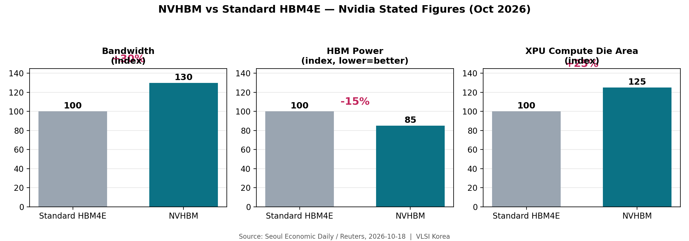
Figures as stated by Nvidia for NVHBM versus standard HBM4E, reported October 2026. Source: Seoul Economic Daily, 2026-10-18
The third row is the one that matters most commercially. Moving the memory controller off the XPU and into the base die frees up to a quarter more area on the compute die — area Nvidia can spend on more compute, more cache, or better yield on the same die size. The bandwidth and power gains are real, but the area transfer is the structural prize: value migrates from the accelerator die into the memory stack, and whoever controls the base die controls where that value is manufactured.
Two models, side by side
| Element | Samsung turnkey (standard HBM4/HBM4E) | NVHBM standardized model |
|---|---|---|
| Base die process | Samsung Foundry 4nm | TSMC 3nm |
| Core die | 1c DRAM (sixth generation) | 1c DRAM (sixth generation) |
| Memory controller | Supplier-side design | Nvidia design, in the base die |
| Validation | Per supplier | One common standard |
| Scope | Standard HBM; custom for AMD and others | Nvidia NVHBM only |
| Status | HBM4 in mass production; HBM4E in production validation | Reported October 18, 2026; no official comment from the three suppliers |
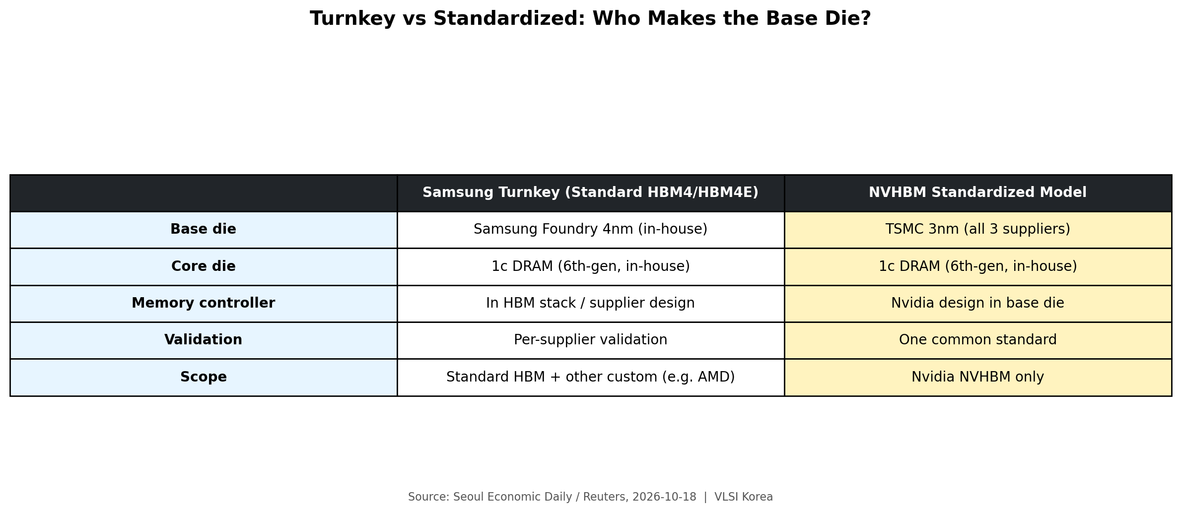
The economics of standardization
Standardization is usually told as a story about the weaker party losing. That framing fails here, for three reasons.
First, the requirement is symmetric. SK hynix and Micron received the same demand. SK hynix was already working with TSMC on base dies, so the adjustment cost falls unevenly — but the rule itself is platform policy, not a verdict on Samsung's 4nm.
Second, what Samsung gives up is narrower than it looks. The base die is one die in a stack of 12 or more core dies. The core die — the actual DRAM, where Samsung's process technology, yield learning and capacity live — stays in-house, on 1c. Samsung keeps the memory value, the stacking, the TSV work and the customer relationship. What moves to TSMC is a logic wafer order for the base layer of Nvidia's custom product only.
Third, what Samsung buys is participation. NVHBM is Nvidia's custom-HBM road map. Being inside it — even on standardized terms — beats being the supplier that held out for turnkey purity and got designed out. In platform markets, the standard is the market.
Make-versus-buy, reversed
The classic make-versus-buy question is asked by the manufacturer. Here it is asked by the customer. Nvidia is effectively unbundling the HBM stack: it standardizes the layer where its own IP lives (the base die) and commoditizes the interface between suppliers, while leaving the layer where suppliers genuinely differ (DRAM core die yield and cost) competitive.
That is supply-chain governance, not procurement. Nvidia reduces its own validation cost, compresses performance variance across suppliers, and increases its switching power — any of the three makers can supply a stack whose base behaves identically. The suppliers, in exchange, get a larger, more predictable custom-HBM market and a shared standard they can plan capacity against.
Samsung's backup-source option
The reporting adds one more detail: Samsung is reviewing its own foundry as a backup source if TSMC capacity runs short. Read carefully, that is not defiance — it is insurance language, and it cuts both ways. It tells Nvidia the supply is de-risked. It also keeps Samsung Foundry in the conversation for the next generation, which is where Samsung's real question sits: not whether TSMC builds this base die, but whether Samsung can win back design leadership of the base die in the generation after.
Chase's Take
The headline writes itself as "Samsung loses to TSMC." That is the wrong story.
The moment the memory controller moved into the base die, the base die stopped being a memory component and became a logic product designed by the customer. Logic products get built where the customer's design ecosystem, PDK maturity and validation flow are strongest. Nvidia was never going to run three different logic flows for one controller design. Standardization was over-determined the day NVHBM was announced in August.
So the turnkey model is not cracking; it is being bounded. Turnkey survives exactly where the supplier still owns the design — standard HBM4 and HBM4E, and custom programs for customers like AMD who do not impose a common base die. It ends where the customer's IP takes over the stack. That boundary, not any single wafer order, is the durable fact of this story.
For Samsung, the strategic question is generational. This round, the base die is TSMC 3nm and the design is Nvidia's. Next round, can Samsung Foundry offer a base-die package — process, controller integration support, HBM co-design — attractive enough that a customer chooses it voluntarily rather than having it standardized away? That is a design-leadership contest, not a capacity contest. Samsung has the pieces: 1c core dies, in-house stacking, and a foundry that already builds its own 4nm base dies at scale. What it needs is to make the base die a product customers ask for, not a bundle they tolerate.
And a note on symmetry: because SK hynix and Micron face the same requirement, "Samsung alone conceded" is factually wrong. All three memory makers just learned the same lesson — in the custom-HBM era, the customer owns the standard.
Implications
- For Nvidia: one validation standard across three suppliers lowers qualification cost and performance variance, and raises switching power. NVHBM's claimed gains (+30% bandwidth, −15% power, +25% XPU area) become a platform baseline, not a supplier differentiator.
- For Samsung: a modest logic-wafer outflow on one custom program, in exchange for staying inside Nvidia's custom-HBM road map with its 1c core die, stacking and capacity intact. Watch whether the backup-source review becomes a real second-source role.
- For SK hynix and Micron: the same standard applies. SK hynix's earlier TSMC base-die work lowers its adjustment cost; Micron must align its base-die sourcing to the same 3nm standard.
- For TSMC: the base die of the AI era's most strategic memory product becomes a 3nm logic order — small wafers, outsized strategic position.
- For investors: the signal to track is not this wafer order but the next one — whether any customer voluntarily specifies a Samsung-built base die in the following generation, and whether NVHBM volumes (starting with Trainium4-class programs) scale as claimed. None of the three memory makers has officially commented; treat the October 18 reporting as reported, not confirmed.
Sources: Seoul Economic Daily, 2026-10-18; Channel News Asia / Reuters, 2026-10. This article is analysis, not investment advice. Figures attributed to Nvidia are the company's stated figures; the three memory makers had not officially commented as of publication.
📩 Subscribe to VLSI Korea
Get our daily semiconductor deep-dives delivered to your inbox first. Free to subscribe.