VLSI Korea
Samsung vs SK Hynix at SEDEX 2026: Two Blueprints for the AI Memory War
At SEDEX 2026, Samsung and SK Hynix both showed HBM4E with identical specs — the spec race is over. Samsung bets on integration (in-house 4nm base die, KRW 360T Yongin); SK Hynix on specialization (HBF, 10x capacity). PIM standardization at the JEDEC Forum is the next battleground.


🆓 Free article · Anyone can read this article for free
30-Second Summary
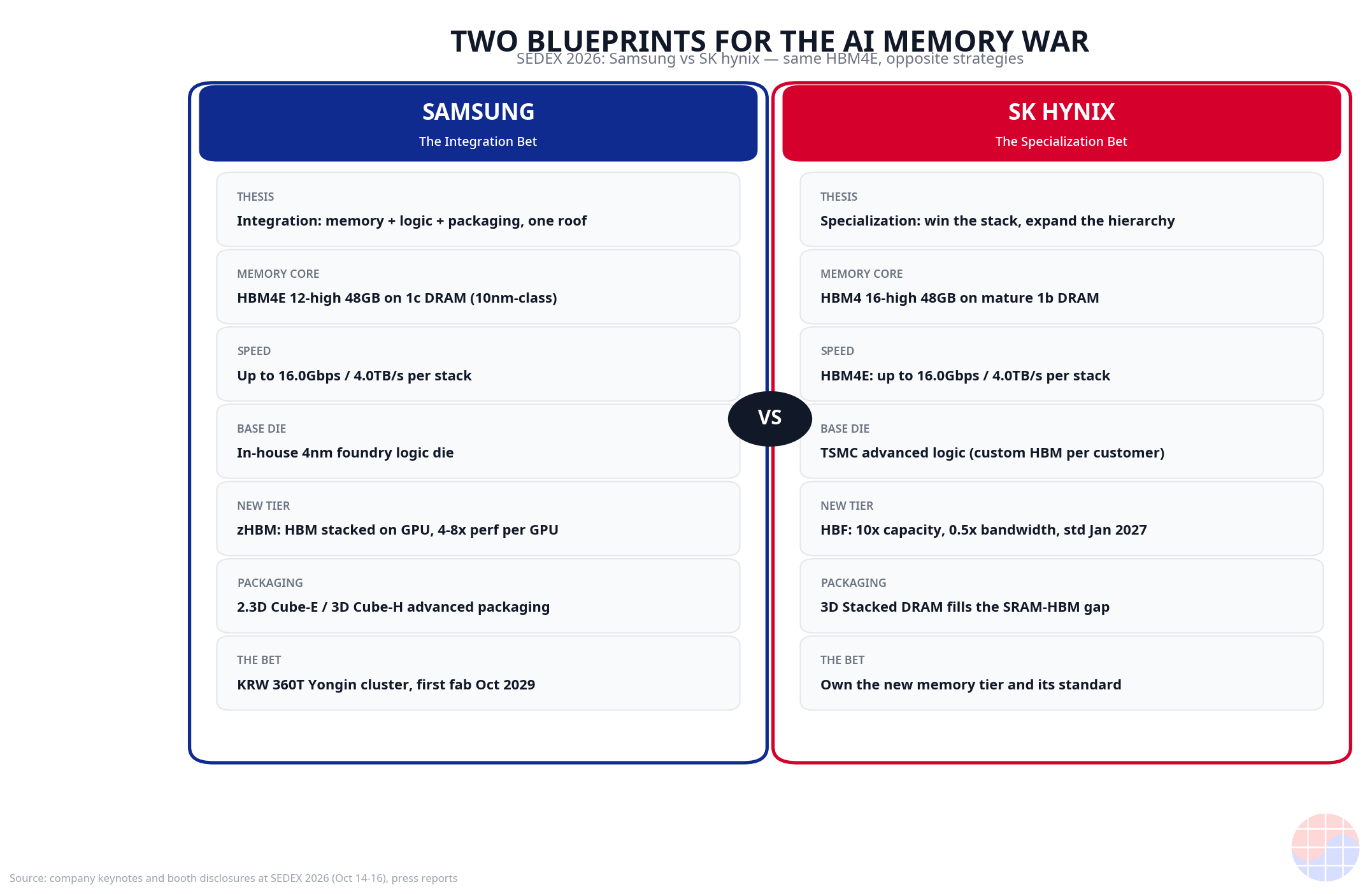
- SEDEX 2026 (Oct 14–16, COEX Seoul) opened as the largest edition in its history: 300 companies, 888 booths. Samsung Electronics and SK Hynix both displayed physical samples of HBM4E, the 7th-generation HBM. Both claim the same headline specs — up to 16.0Gbps per pin, up to 4.0TB/s bandwidth, 48GB in a 12-high stack. The spec race ended in a draw.
- The real contest is elsewhere. Samsung's thesis is integration. DS Division CTO Song Jai-hyuk declared Samsung "the only company in the world that covers DRAM, logic chips, CMOS image sensors, and packaging" — building HBM4's base die on its own 4nm foundry process.
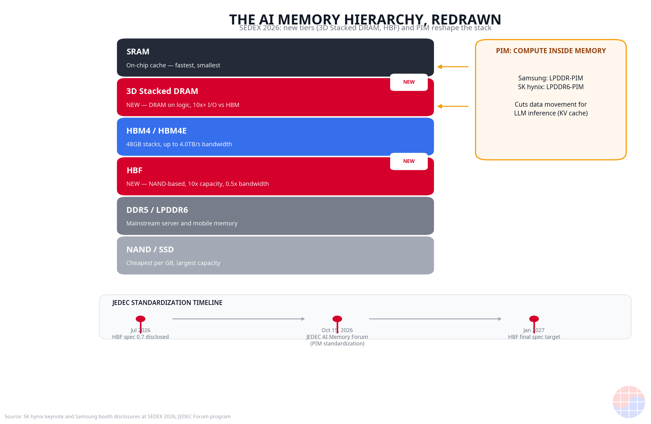
- SK Hynix's thesis is specialization plus hierarchy expansion. Chief Development Officer Ahn Hyun declared that "HBM alone cannot handle surging AI memory demand," unveiling HBF (High Bandwidth Flash) — a new memory tier targeting more than 10x the capacity of HBM. Final HBF specifications are targeted for January 2027.
- The battlefield where the two strategies collide is PIM (Processing-in-Memory). Samsung pushes LPDDR-PIM; SK Hynix counters with LPDDR6-PIM. Both will argue their case at the JEDEC forum at COEX on October 15 at 1 PM.
- Samsung unveiled plans for the Yongin national industrial complex: roughly KRW 360 trillion in investment, construction starting 2027, first production line targeted for October 2029 — the physical proof of the integration thesis.
- Investment takeaway: the HBF standard (January 2027), customer-by-customer custom HBM splits, and PIM standardization leadership will decide the memory value chain for the next five years. (Source: Ajunews, Source: Nocut News)
Background: Same HBM4E, Opposite Stories
Korea's largest semiconductor exhibition, SEDEX 2026, opened on October 14 at COEX in Seoul. Organized by the Korea Semiconductor Industry Association and now in its 28th year, the show runs under the theme "Into the Era of Silicon Intelligence" with 300 companies across 888 booths — the largest edition ever. (Source: Dailian)
The most visible duel sits near the entrance: Samsung and SK Hynix both put 7th-generation HBM4E samples front and center. Samsung shipped the world's first 12-high 48GB HBM4E samples — built on 1c DRAM with a 4nm logic die — in May, and SK Hynix completed sample shipments of its own 12-high 48GB HBM4E after a June reveal at Computex. Both have sampled to NVIDIA. (Source: Herald Business, Source: Dailian)
What is striking is that the spec sheets are effectively identical. Both vendors claim up to 16.0Gbps per-pin speed, up to 4.0TB/s of bandwidth, and 48GB of capacity (twelve 32Gb dies). Samsung disclosed two operating points — 3.6TB/s at a stable 14Gbps and 4.0TB/s at maximum drive — while SK Hynix emphasized energy efficiency improved more than 20% over its predecessor. (Source: IT Chosun)
Identical specs mean the axis of competition has shifted. The contest is no longer "who is faster" but "who defines the memory architecture of the AI era." The opening-day keynotes from both companies' technology chiefs made that explicit.
Business Deep Dive
1. Market structure: an oligopoly, and what a spec draw means
The global HBM market is effectively a Korean duopoly. SK Hynix led through the HBM3 and HBM3E generations with a majority share, while Samsung is chasing with the most advanced process node — 1c DRAM — in the HBM4 generation. That both reached identical headline specs on HBM4E signals a new phase: specs alone no longer differentiate.
When specs converge, vendors have two moves. One is to sell the system beyond the spec; the other is to create a new tier beyond the spec. Samsung chose the former. SK Hynix chose the latter.
2. Samsung's thesis: integration — "the only company"
Samsung DS Division CTO Song Jai-hyuk used his keynote to state that Samsung is "the only company in the world that covers DRAM memory, logic chips, CMOS image sensors, and packaging." This is not boothmanship; it is a business-model declaration. (Source: TechTimes)
The substance of the integration thesis is the base die. The base die — the bottom layer of the HBM stack that manages data traffic between the DRAM layers and the GPU — has become a full system-logic die starting with the HBM4 generation. Samsung builds it on its own 4nm foundry process, combining the memory core die (1c DRAM), logic design, base die, and advanced packaging under one roof. That enables memory-logic co-optimization no external-foundry customer can easily replicate — and keeps the margin inside.
The booth lineup backs the thesis: LPDDR-PIM (compute inside memory), zHBM (a mockup of a 3D memory architecture stacking HBM directly on the GPU), zNAND-O (a mockup of a 3D NAND solution for edge AI), 2.3D Cube-E (silicon-bridge-based expandable packaging), and 3D Cube-H (3D packaging) — literally "Architecting AI Systems," the booth's theme. zHBM targets 4–8x performance per GPU and up to 3x performance per watt versus HBM4E; zNAND-O targets up to 7x read bandwidth and energy efficiency versus conventional NAND. (Source: IT Chosun, Source: Ajunews)
And the physical proof of the integration thesis is the Yongin national industrial complex. Samsung plans to invest roughly KRW 360 trillion, begin site preparation and construction in 2027, and bring the first production line online in October 2029, with around 70 materials, components, equipment, and fabless companies moving in. Integration stops being a design philosophy and becomes real land, real money, and a real supply chain. (Source: Ajunews)
3. SK Hynix's thesis: specialization plus hierarchy expansion — "HBM alone is not enough"
SK Hynix Chief Development Officer Ahn Hyun titled his keynote "Asking About the Direction of Memory Innovation in the AI Era." His core diagnosis: the KV cache bottleneck. As AI inference grows more complex and context windows lengthen, the key-value cache storing previous tokens exhausts HBM capacity before bandwidth becomes the limit. Ahn projected AI infrastructure performance scale expanding roughly 20x by 2030 versus 2026. (Source: Dong-A Ilbo, Source: Nocut News)
The fix is not faster HBM but a redesigned memory hierarchy. Ahn's roadmap has three branches.
First, HBM advancement and customization. After HBM4E, SK Hynix will pursue HBM5 and custom HBM4E in parallel in 2027. Custom HBM embeds customer-specific logic IP in the base die, tailoring memory to each AI accelerator — with the base die built on TSMC's advanced logic process. A memory company internalizing logic design while outsourcing manufacturing to the best foundry: specialized division of labor. (Source: IT Chosun, Source: Korea JoongAng Daily)
Second, 3D Stacked DRAM — a new tier between SRAM and HBM, stacking DRAM dies directly on logic chips (GPUs, NPUs) to shrink data-travel distance, with I/O scaled up dozens of times over conventional HBM. Conceptually adjacent to Samsung's zHBM, but positioned as one axis of a full hierarchy roadmap. (Source: Prime Economy)
Third, the boldest move: HBF (High Bandwidth Flash). SK Hynix is applying the TSV stacking and high-speed I/O technology accumulated in HBM to NAND flash, creating a new memory tier between HBM and DRAM. The development target: roughly half the bandwidth of same-generation HBM at roughly 10x the capacity, placing large repeatedly-read datasets close to compute for AI inference — a workload where reads vastly outnumber writes. Spec 0.7 was disclosed in July 2026; the final specification is targeted for January 2027, with standardization pursued alongside global partners including SanDisk. (Source: Nocut News, Source: NSP News, Source: Dong-A Ilbo)
4. PIM: where the two strategies collide
The point of direct collision is PIM. Samsung displayed physical LPDDR-PIM; SK Hynix answered with LPDDR6-PIM. Both rest on the same diagnosis — that inference bottlenecks are about data movement, not compute — and both chose in-memory compute as the card to play. (Source: Global Economic)
The rulemaking venue is the JEDEC Forum ("Industry Forum on AI Memory Architectures, Testing, and Ecosystem Readiness"), convening at COEX Hall C on October 15 at 1 PM. Samsung will present LPDDR-based PIM for LLM inference bottlenecks; SK Hynix will present LPDDR6-PIM for on-device AI and JEDEC standardization trends. Advantest (HBM bump testing), Keysight (DDR6/LPDDR6 testing), Synopsys (server memory), Intel (on-device AI memory), and MediaTek join. Whoever writes the standard governs the ecosystem — this is not a technical seminar but the venue deciding AI memory architecture leadership for the next five years. (Source: Newspim, Source: Newsis)
5. Reading the two bets through cost structure
The two strategies park risk on different layers. Samsung's risk is process risk: the 1c DRAM plus 4nm base-die combination must ride the yield curve, and it ties into foundry utilization. SK Hynix's risk is stacking risk plus standards risk: 16-high stacking multiplies per-layer yields so bonding precision is existential, and HBF only works if the standard pulls an ecosystem in — the SanDisk partnership is the hedge.
There is a shared headwind. Tesla CEO Elon Musk recently complained publicly about memory prices on social media — a signal that Big Tech customers are starting to feel memory is "too expensive." The stronger the oligopoly's pricing power, the harder customers will push back through custom HBM and standardization. That is precisely why both companies are chanting "custom" and "standards" at once. (Source: Dong-A Ilbo)
Chase's Take
Two companies holding up the same HBM4E sample and telling opposite stories — that is the state of this industry. When the spec race ends, what remains is the right to define the architecture. Samsung says "we do everything, so use our architecture." SK Hynix says "the hierarchy is expanding, so we write the new tier's standard." Both have a point. As AI workloads shift weight from training to inference, capacity (the KV cache) and system integration (base die plus packaging) matter simultaneously.
From the Korean vantage point: Samsung's KRW 360 trillion Yongin bet and SK Hynix's HBF standards play are two sides of one coin. Both are playing the standards-and-ecosystem game. Yongin builds the integrated ecosystem in physical space; HBF builds the new tier's ecosystem in standards space. Korea's next decade in memory will be decided not by who stacks higher, but by who pulls more partners inside their tier and their standard.
Verification and counterpoints are in order. First, HBF's "10x capacity, half the bandwidth" is a development target, not a shipping spec — partner adoption after the January 2027 spec freeze is the real test. Second, custom HBM margins depend on the design-split with customers (accelerator designers like NVIDIA): who designs and who builds the base die is where the power sits. Third, PIM has been discussed conceptually for over a decade. Whether JEDEC standardization converts into real product adoption this time is the question — holding the forum is not itself a victory.
Implications: Investment and Management Takeaways
- Memory investors: The HBM4E spec draw is already priced in. The next catalysts are (1) the HBF final spec (January 2027) and partner adoption, (2) customer-by-customer custom HBM order splits, and (3) PIM standardization leadership. Yongin's first fab (targeted October 2029) is the yardstick for Samsung's medium-term capacity visibility.
- AI accelerators and Big Tech (memory buyers): Oligopoly pricing power is at a peak. Multi-sourcing and co-designed custom HBM are the key levers for pricing power. If HBF standardizes, inference-infrastructure memory TCO changes — time to reflect it in architecture roadmaps.
- Equipment and materials: 16-high-era TC bonder precision, HBM bump testing (Advantest), and DDR6/LPDDR6 testing (Keysight) demand grows with standardization. Yongin's 70-company move-in plan is a barometer for domestic equipment makers' medium-term order books.
- General management: The duel between the standards-setter and the integrator is not just a memory story. In any industry, choosing between "creating a new layer" and "integrating everything" is the classic platform-strategy fork.
FAQ
Q1. How does HBM4E differ from HBM4? A1. HBM4E is the 7th-generation HBM, an extension of HBM4. Both Samsung and SK Hynix target up to 16.0Gbps per-pin speed, up to 4.0TB/s bandwidth, and 48GB capacity (twelve 32Gb dies). Samsung uses a 1c DRAM core with an in-house 4nm base die; SK Hynix uses a mature 1b DRAM process with a TSMC logic-process base die. Both sampled to NVIDIA in 2026.
Q2. Is HBF a replacement for HBM? A2. No. HBF (High Bandwidth Flash) is a new memory tier sitting between HBM and DRAM, not a replacement. It applies TSV stacking and high-speed I/O to NAND flash, targeting roughly half the bandwidth of same-generation HBM at roughly 10x the capacity — for large repeatedly-read datasets like inference KV caches kept close to compute. The final specification is targeted for January 2027.
Q3. Why did PIM suddenly become important? A3. Because AI inference bottlenecks turned out to be about data movement, not compute (GPU FLOPS). In LLM inference, moving weights and KV caches between memory and compute costs time and power. PIM performs computation inside memory, cutting that movement. Samsung pushes LPDDR-PIM and SK Hynix LPDDR6-PIM, with standardization trends on the agenda at the October 15 JEDEC Forum.
Q4. What does Samsung's KRW 360 trillion Yongin investment mean? A4. It is the physical proof of the "integration" strategy — memory, foundry, and packaging in one place. Samsung plans roughly KRW 360 trillion for the Yongin national industrial complex, with construction starting 2027 and the first production line targeted for October 2029, hosting around 70 materials, components, equipment, and fabless companies. The integration thesis moves from design philosophy to real capacity and supply chains.
Written on October 15, 2026, from public sources. Roadmaps cited (HBF specifications, PIM standardization) are each company's development targets and subject to change. Not investment advice.[^1]
[^1]: Limits of evidence: figures cited were cross-checked across press reports and company announcements; outcomes of the JEDEC Forum (convened October 15) were not yet public at the time of writing and are not included.
Related reading
- The Post-HBM Memory Hierarchy War: SK Hynix vs Samsung Battle to Define…
- Daily Silicon: Samsung, SK hynix: KRW 43.2T HBM, DRAM Facility Spend
- Daily Silicon: AMAT WFE Guide to 30%+, Foxconn AI Server Surge, Hynix…
- HBM4: Micron vs SK hynix vs Samsung
- Daily Silicon: SK hynix CPO and HBM: $97.94B in AI Chip Orders
- SEDEX 2026 Opens Tomorrow: HBM4E, HBF Debut, and 5 Things to Watch in Seoul