
It used to be that "how many nanometers of process or how many cores" seemed to describe most of the performance of semiconductors.
Nowadays, words like chiplet, 2.5D, 3D IC, and UCIe are the first things you'll hear.
It's not just because they're buzzwords.
A startup has beaten Nvidia to the punch, but... No other semiconductor can beat Nvidia's performance + power + ubiquity + mass production yields in the broader marketplace.
The graph below was compiled by Amir from riselab.
Black is the performance improvement slope for system semiconductors > Memory semiconductor performance improvement slope > Interconnect performance improvement slope
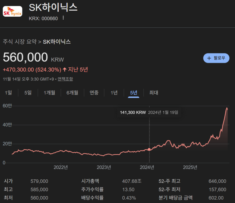
HBMs have been driving the stock prices of SK Hynix (the world's top technology company), Samsung Electronics (the world's top production company), and Micron (the top memory company in the U.S.) to skyrocket recently.
But... The only thing slower than memory is the interconnect.
I used to think "Chiplet = big chips cut into pieces and glued together", but the more I look into it, the more I realize that the next semiconductor game will be won or lost by the interconnect.
The process is better, so why split the chip
To talk about Chiplet, we need to start with "why did we abandon monolithic SoCs?"
First, Reticle Size Limitations.
We draw schematic masks with an exposure machine (ASML), and there is a maximum area that this machine can draw a circuit. If you design a high-performance CPU, GPU, and AI accelerator on one giant die, you'll be near this limit. Beyond this point, the design itself becomes more complex and yields drop dramatically.
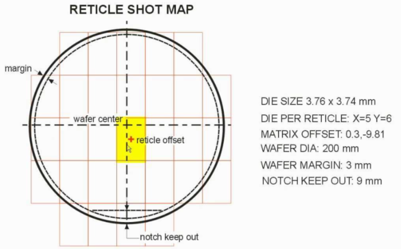
Second, yield and cost structure.
The larger the area, the greater the loss from "one bad one". If you have a single piece of dust in an 800 mm² die, the whole chip is bad and you have to throw it away, whereas if you have four 200 mm² pieces, if one is bad, the other three can be used for other combinations. Statistically, the chiplet structure is much more favorable. The finer the process, the higher the cost of a die, so the difference is felt more strongly.
https://semiengineering.com/designs-beyond-the-reticle-limit/
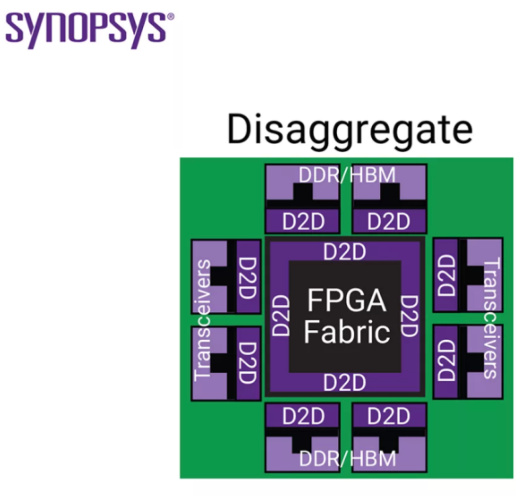
Third, Heterogeneous Integration.
Today's SoCs have CPU, NPU, GPU, High-Speed SerDes, DDR/LPDDR/PHY, analog, RF, power management, and more. It's not always best to implement every block in the latest FinFET/GAA process. Digital logic benefits from leading-edge processes, but analog and I/O are more reliable and cheaper on mature processes."
The end result is "make each block on the best process, and then combine them in a package. The key words here are 2.5D, 3D ICs, and chiplets."
To summarize, chiplets are "a structure for bypassing process limitations, controlling yield and cost, and mixing different processes in a single package. The problem is, once you've broken it down, it's much harder to figure out how to connect the dots.
But... Chiplet looks good because of the yield and cost structure,
but the manufacturing process for 2.5D ICs and 3D ICs is complicated, so the yield can be low, and you need to spend a lot of money to compensate for it, so you may end up with a bigger belly than your stomach.
That's why we don't see a lot of mass production yet.
On-Die Wire to Die-to-Die Link
In a monolithic SoC, most of the data flows on top of the on-die metal layer. Even global wires are still wires on silicon, sending and receiving signals with hundreds of ps to a few ns of delay and relatively low energy.
While Network-on-Chip (NoC) design is important, the physical routing itself is more of a "do it in the chip" problem.
The moment you get to the chiplet structure, you have critical data going out of the die and coming back in. In other words, the path changes like this:
Core → On-Die NoC → Die Edge → Micro Bump → Interposer or RDL → Micro Bump on another die → On-Die NoC → Core
From a physics perspective, a few things change.
The medium of the wiring changes
Now we're not just dealing with a metal layer on silicon, but we're passing through a variety of media, including micro bumps, TSVs, silicon interposers, fan-out RDLs, and organic substrates.
Length and environment change
It's much longer than on-die wire, and the impedance is more complex. Signal integrity issues come into play. The "wall" between traditional package SerDes and on-die wire is broken down, and very advanced SerDes design-level concerns are brought into the package.
The price of energy and area is different
The cost of adding one more on-die wire is not the same as the cost of adding one more die-to-die link. The length of the die edge is limited and the bump pitch is limited. As you increase the number of links, the die perimeter area, PHY cell area, routing, and power are all impacted.
Routing
What used to be a "we can use a little more wire" design is now a "is this link really worth the bandwidth?" design.
From this point on, the interconnect is not just physical wiring, but a key resource that determines the architecture of the entire Chiplet System.
Chiplet Interconnect from a PPA perspective
At the end of the day, every design comes down to PPA (Power, Performance, Area) and Cost. Chiplet Interconnect is deeply involved in all four pillars.
Performance: Bandwidth and Latency
Tons of data flows between AI accelerators, GPUs, high-performance CPUs, and high-bandwidth memories like HBMs. When this data flows over a die-to-die link, rather than on-die, the bandwidth density and round-trip latency of the link sets the upper limit on system performance.
If there is not enough bandwidth, no matter how many cores you add, you will hit a "Memory Wall". And if the latency is too high, fine-grain collaboration becomes difficult and the architecture must be designed with coarse-grain. For example, if the L3 Cache is separated into chiplets and the latency is too large, it becomes almost like off-chip memory.
Power: Fighting for pJ/bit
On-Die Wire can compress power down to tens of fJ/bit, but Package-Based SerDes often cost several pJ/bit. Short-reach, ultra-low-power PHYs for chiplets are also aiming for sub-pJ/bit, but they are still more expensive than on-die."
At the end of the day, as a system architect, you have to ask yourself, "Do I really want to send this data across the die, or do I want to compute it once more on the die and compress it? As the power price tag of the interconnect changes, the Compute vs Communication Trade-Off changes as well.
Area: Die Edge and PHY Area
Chiplet Interconnect is "Edge-Centric". Bump and PHY are placed along the die perimeter. Increasing the die size increases not only the core area but also the edge length, but how efficiently the edge is allocated to the interconnect directly affects the PPA.
Particularly when using a standardized die-to-die interface such as UCIe, the area occupied by the PHY, controller, and protocol stack cannot be ignored. Reducing the area and power required here is the competitive advantage of chiplet design.
Cost: Process mix and package complexity
With a chiplet structure, you can reduce die unit cost by splitting logic into leading edge processes and I/O into mature processes. The problem is the package cost. Silicon Interposer, high-density RDL, and fine-pitch bump are very expensive. Excessive interconnect requirements complicate the package structure, which in turn drives up the overall cost.
So interconnect becomes the barometer for "does this chiplet architecture make economic sense?"
UCIe, and the Standardization of Die-to-Die Interfaces
One of the most talked about keywords these days is UCIe (Universal Chiplet Interconnect Express). While the name has a PCIe feel to it, it actually aims to provide compatibility with existing protocols such as PCIe/CXL, as well as PHYs specialized for die-to-die environments.
The reason for UCIe is clear. Chiplets from different companies can be combined
The chiplet ecosystem would never grow if each company stuck to its own proprietary die-to-die interface. It is only when there is a "standard interface that anyone can combine" that we can truly have "prefabricated" designs at the SoC level.
The benefits of standardization are obvious: for example, one company can make a CPU chiplet, another an NPU chiplet, another a SerDes/IO chiplet, and a system company can combine them into a package. Of course, in reality, it's not that simple due to IP, validation, and liability issues. But just the fact that it's a "possible scenario" is a big change.
EDA and Design Flow are cleaned up
Rather than having to model new proprietary PHYs and protocols every time, UCIe-based channel and link models can be used as a common foundation. There is a common denominator for STA, SI, PD, and Package Co-Design Flow.
On the flip side, having a standard also means that "the interconnect itself becomes a point of competition". The company with the PHY IP, Package structure, and Co-Optimization technology that can make power/bandwidth/delay/area better will have an advantage in the market.
The blurring of package and chip design
Another reason Chiplet Interconnect is so important is that it blurs the "design boundaries".
In-die: Logic Design, Physical Design, STA, On-Die SI
Package: Designed by PCB/Package Team separately and at much lower speeds
In a chiplet structure, the two are completely indivisible. The channels in the Die-to-Die Link look at both package and die edge structures simultaneously. Die placement, bump mapping, interposer routing, package stack-up, and PHY placement inside the die must be considered at once."
At the end of the day, these questions are addressed by a team.
How far apart are A and B chiplets
How much channel length can we tolerate on the interposer
What order do we place the bumps on the die edge
Where do we boundary the On-Die NoC and Die-to-Die Link
This is where the Package Engineer, PD Engineer, SI Engineer, System Architect, and EDA Tool Vendor sit at the same table.
As chiplets become more widespread, the perspective required of designers will change:
Not just "understanding a few nanos of the process,"
The ability to understand the physical, logic, and protocol layers of the interconnect together
The system-level view of the on-die NoC and off-die fabric as an integrated whole
The ability to analyze end-to-end trade-offs, including power/area/cost
These three things will become increasingly important.
You may be thinking, "There's still a lot to do with transistors, logic, PDs, and STAs, and then there's the interconnect and package." But it's better to go into the design knowing at least "where the real bottlenecks are that determine chip performance and cost". These days, that bottleneck is very often the interconnect."
From my perspective, interconnect in the chiplet era is not a topic to be avoided, but rather a great opportunity to expand your career. The moment you understand die-to-die and package, you become a "whole chip" person, instead of just looking at timing and SI in the die. The scope of what you can do is much broader."