
One of the most frustrating bugs after semiconductor tape-out is this one:Function simulation is perfect, Silicon Bring-up works most of the time, but "sometimes" it behaves erratically. When I try to reproduce it in front of a professor, it works fine.... The debug logs are also faint due to the lack of reproducibility. If you dig deep enough, you often come to the same conclusion:
- "Timing is broken somewhere."
- That "somewhere" is often a global control like Clock/Reset.
- Specifically, a very thin pulse (glitch) at the Clock to MUX point.
Glitches in the clock path are a different class of glitch than data glitches. Glitches in the data path are usually consumed in combinational logic.
Clock glitches, on the other hand, can be perceived by the flip-flop as an "extra clock edge", and from that moment on, one abnormal edge can distort the entire system state. This is why the classic solution is the Glitch-Free Clock MUX (GFCM).
1) Why Glitch occurs in a regular Multiplexer (MUX)
The simplest 2:1 The logic of a MUX is clean.
out = (~S & A) | (S & B)In RTL, it looks like it changes from A to B as soon as sel goes from 0→1.
At the gate level, it's a different story.
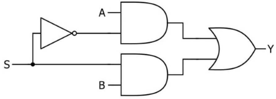
- (~S & A) and (S & B) paths have different cell delay / wire delay.
- S's signal propagation does not arrive at both paths simultaneously.
- In that short gap, the OR input combination changes briefly, causing signal switching for a short time. (static hazard / dynamic hazard)
In a clock MUX, A and B are usually asynchronous clocks. Since the phase relationship between A and B is not fixed, the probability of the sel transition being caught at a "bad moment" is higher than expected, resulting in a silicon bug that fails "sometimes".
2) Why Clock Glitch is necessary
- Pulse width can be recognized as a clock by FF even if it is short
Slew/threshold in the clock tree, Depending on the internal pulse filtering of the library FF, "unwanted edges" can validly enter. - Easy to break setup/hold at the same time
If a glitch is attached just before a normal edge, it will break the hold; if it is attached immediately after, it will break the setup. Either way, the result is random. - In the era of DVFS/Fail-over/Power domain, clock switching is commonplace.
3) Glitch-Free의 핵심 정의: "Sealing transition conditions", not "Glitch 0"
The key to a Glitch-Free Clock MUX is simple.
No clock edges pass through while changing the output clock;
The select signal (Enable) only changes during the stable part of the clock;
One important insight here:
GFCMs are often pause-enabled circuits rather than seamless circuits.
This means that the price of being glitch-free may be missing a cycle or two. This should be specified in the design specification." If "glitch-free" switching is the goal, it should not just be a matter of changing the MUX, but should be approached at the PLL/clocking architecture level.
4) 가장 널리 쓰이는 구조(정석): "Mutual-Exclusion + Safe-Window Update"
If the glitch is too close to the old clock, it will cause a timing violation.
To avoid this, we need logic to pause the clock toggle for a while.
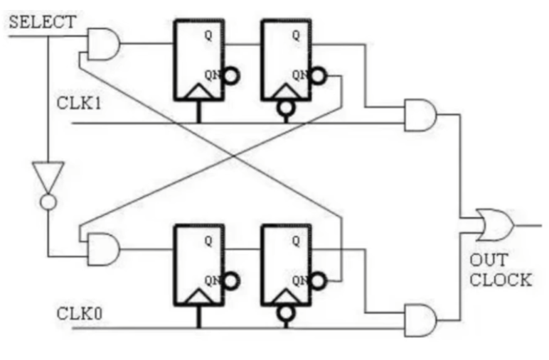
If you look at the front and back parts, it is the same structure as a MUX,
- There is a two-stage synchronizer inside,
- There is a feedback loop that synchronizes to the opposite clock when the SELECT signal changes.
In the end, it does the following.
- enable1 and enable2 don't go to 1 at the same time (mutual exclusion)
- turn off one before turning on the other (break-before-make)
We stop the clock briefly during the transition, and open the other only on the safe side.
Electronicspedia channel has a very good example of a Glitch, so I've attached it:
5) "Glitch vs Glitch-Free" in waveform (core only)
(1) naive MUX (Glitch can occur)
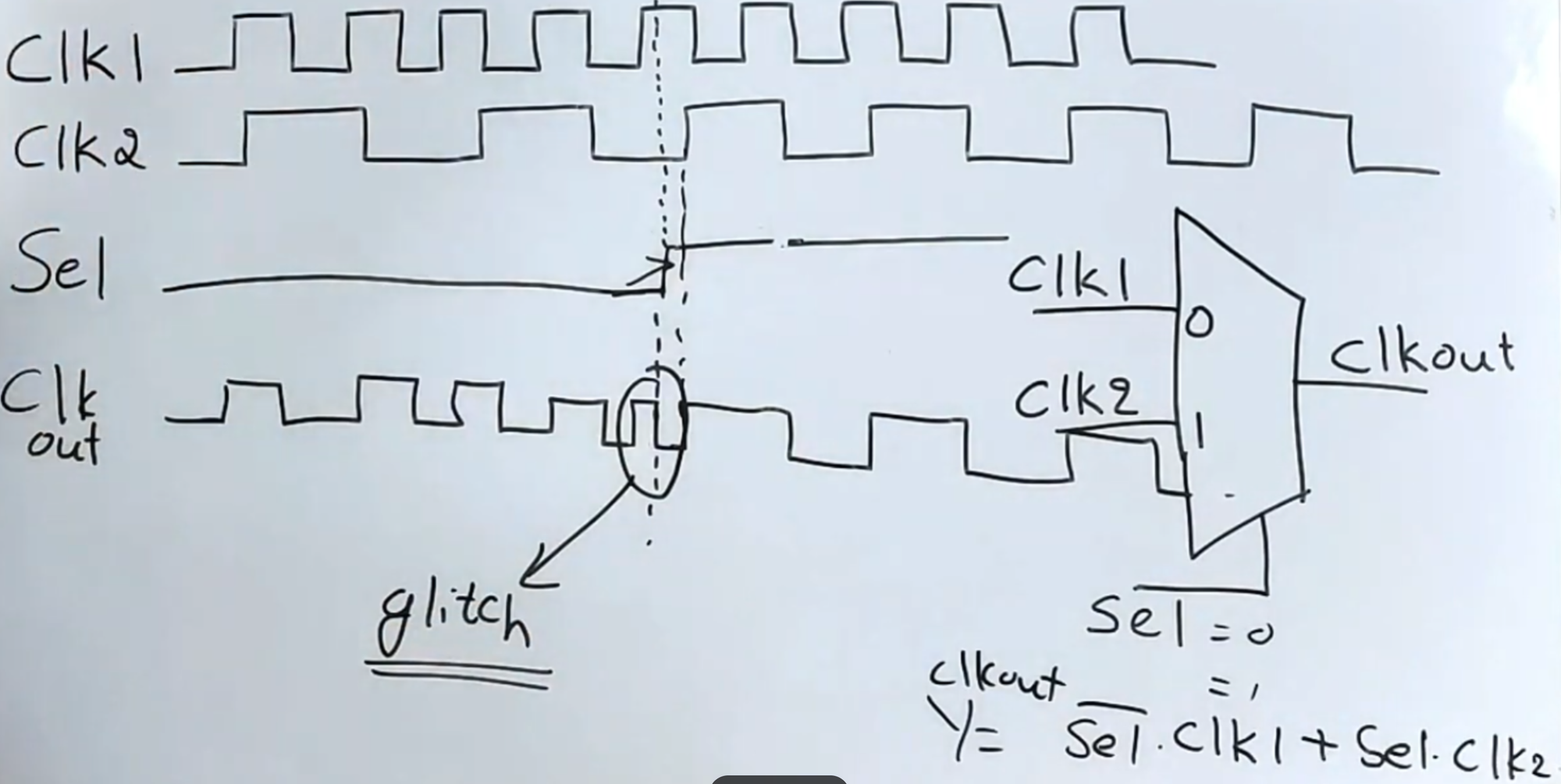
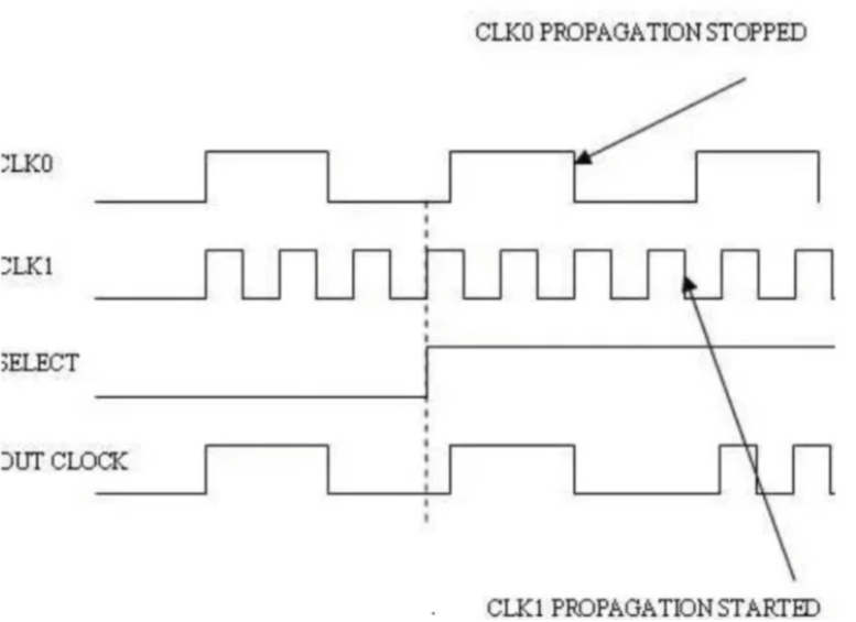
As shown in the figure,
When Sel is 0, CLK1 is output, and when Sel is 1, CLK2 is output.
The clock toggle that Designer didn't want to happen, like the dotted part of CLK Out, is called a glitch:
6) In SDC and CDC analysis:
The Clock MUX output is "both CLK1 and CLK2". So it is common to define two overlapping generated clocks for the output pin, and exclusive indicates that both generated clocks cannot be active at the same time.
- The sync FF inside the GFCM is CDC, so check the functional safety separately with a CDC tool (SpyGlass-CDC, etc.).
7) CTS/PnR 인사이트: GFCMs are not "logical blocks", they are "Clock Root devices"
GFCMs are of varying quality depending on their placement. This is especially true in advanced nodes:
- As close to the clock source (PLL/OSC) as possible: Longer clock nets before and after the MUX increase SI/EM/IR-drop impact and skew management difficulty:
- Select/control is control, not data: As fanout grows, glitch-free structures increase "transition delay". If you give this path a set_case_analysis, you may find a very large violation in gate level simulation. This needs to be managed so that constraints can be imposed:
- Separation of roles from CTS: The real clock tree is after the output of the GFCM:
- Duty cycle / pulse integrity: Simple AND/OR gating can create duty distortion. Prefer foundry-qualified cells rather than just creating GFCMs in RTL.
In a nutshell:
GFCMs should be treated as part of the clocking architecture and are "protected" in PnR.
8) DFx(Scan/ATPG/Bring-up) 관점: GFCM is the "door to testing"
Scan usually has different shift clock and capture clock demands, and at-speed tests are more demanding. Here's how a poorly designed GFCM breaks DFx:
- scanning stalls because clock switching is not allowed in test mode
- pauses in the capture section, breaking the pattern
- glitches in the reset/test_en transition, causing it to malfunction
So the working pattern is usually this.
- Directly bypass test_clk with test_en (like in RTL above)
- Or have a separate clock mux for scanning, separate from the function clock mux
Some experts make only glitch free clock muxes like this one!
Describing the Glitch-Free Clock MUX as a "glitch-free mux" is too thin.clocking infrastructure that runs through DVFS/Fail-over/Power domain/DFx.
This small block reveals the maturity of the design:
- Student designs look at "does the RTL make sense"
- Junior designs look at "does the STA pass"
- Senior designs look at "is it mass-producible"
.