
In advanced processes, the process name (e.g., 7nm, 5nm, 3nm) does not correspond to the actual physical dimensions. Instead, chip manufacturers use them to differentiate generations for marketing purposes, highlighting performance improvements to consumers.
In reality, recent process node names no longer refer to any specific circuit dimension. By the late 2010s, they had become mere generational labels.
In other words, the name "3nm process" no longer signifies a 3-nanometer structure; it is a marketing name implying that the PPA level is at the 3nm class.
Consequently, to truly evaluate whether a process is "finer", alternative metrics based on geometric characteristics (font size, pin size, etc.) must be used instead of traditional nm units.
The most important factor is PPA. Even if the process level isn't fine, if it's mass-producible and has good PPA, it's a good process. However, this article only addresses methods for determining process fineness. It does not cover PPA.
What does it mean for a process to be fine?
This article uses the size of devices (FEOL, BEOL) and the spacing between device placements as criteria.
Geometric Resolution Definition
The resolution of a process is ultimately determined by the minimum dimensions of devices or interconnects.
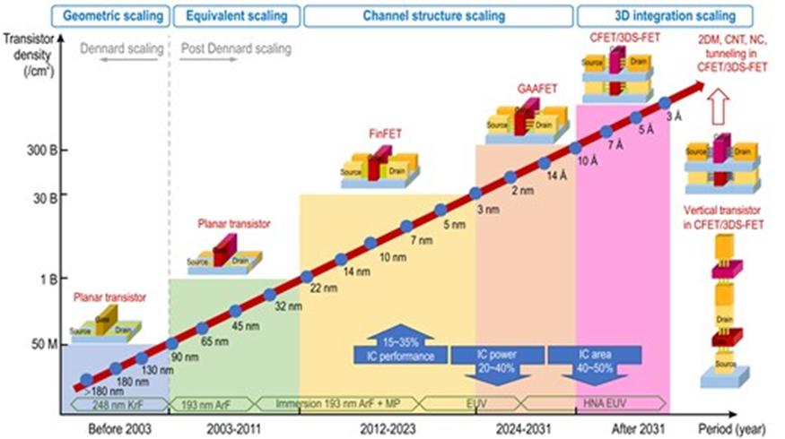
This is called Geometric resolution. Specific metrics include various items such as Contacted Poly Pitch, Metal Pitch, fin pitch, sheet pitch, and Via Pitch.
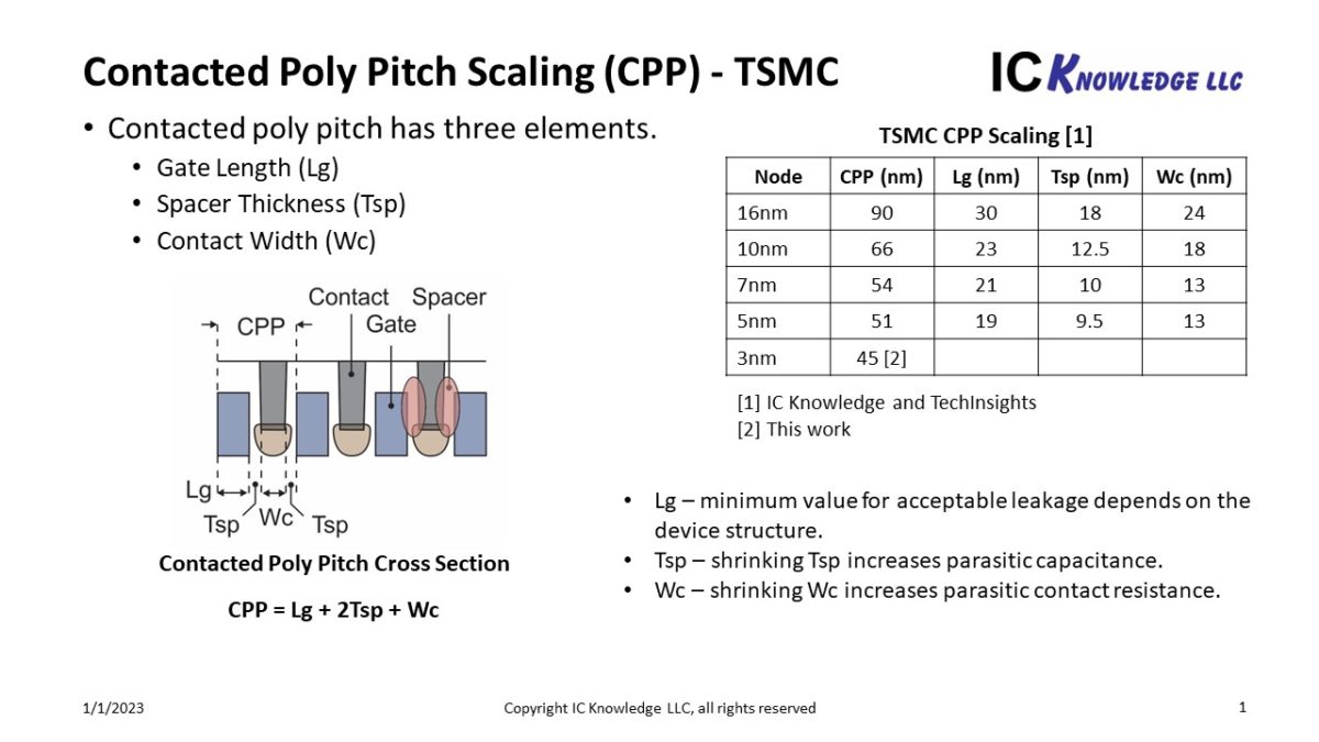
- CPP refers to the gap between one transistor gate and the next, often also called the transistor Gate pitch.
- MMP is the sum of the minimum metal line width and spacing, typically equal to or slightly larger than the front-end metal(M0 or M1) pitch or slightly larger.
- In FinFETs or GAAFETs, the fin pitch or sheet pitch determines the channel width. In the latest processes (e.g., TSMC 5nm), the fin pitch is known to be around 25nm.
- Gate Pitch, Track Height: These metrics determine the height of a standard cell. Besides CPP, the number of cell tracks (n-track cell) and cell height can also serve as alternative indicators. For example, in a 5nm process, one might refer to a 6-track cell with a 180nm cell height. Considerations must also include cases where same-net spacing is permitted between layers on the same network in the layout, and exceptions must be made for line-end spacing differences based on line-end shapes.
- TSMC's 5nm process is estimated to have a CPP (Poly pitch) of approximately 48nm and a metal pitch of around 30nm.
- Meanwhile, Intel's "7nm" process (Intel 4 Process) is known to have a CPP of 50nm and a fin/metal pitch of 30nm.

By synthesizing these metrics, a practical comparison chart of process fineness can be created.
For example, TSMC's 3nm (N3) node was publicly announced with a CPP of 45nm, and even compared to other nodes, there is a significant gap in transistor gate pitch and fin pitch.
‘nm’ The History and Marketing Background of the Naming
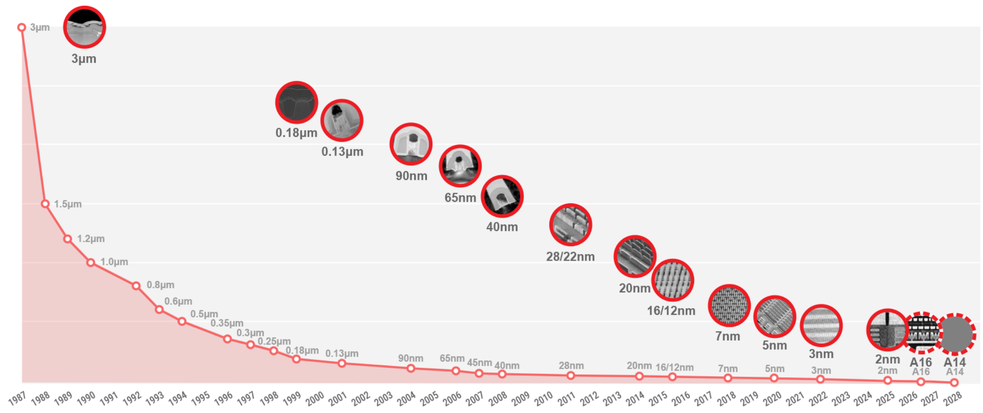
In the early days, process names were directly linked to the minimum dimensions of the process
In other words, whenever names like 22nm, 14nm, 10nm, or 7nm were introduced, it didn't mean all devices or wiring were uniformly scaled down. Instead, the name simply continued to signify an overall generational shift in that process.
In reality, the 7nm process of one major foundry achieved a level of integration comparable to a competitor's 10nm process. Moreover, the actual geometric size of that competitor's 10nm process was larger than 10nm.

As node names became independent of physical dimensions, questions like "Is Company A's 2nm really finer than their 3nm?" or "Isn't it just 2nm, not 3nm?" were frequently raised. Isn't it just a second-generation 3nm?" Thus, even if a specific foundry claims to have the world's first *nm process, the actual integration density and PPA often fall short of competing foundries.
Each metric can be indirectly inferred from process technology literature or presentation materials.
If you have obtained the PDK, you must extract this dimensional information from the DRC Rules or Technology LEF files. If Poly min width and Poly min spacing are available, you can calculate the CPP.
Data Sources and Reliability Priority
- Design Rule Deck: The DRC Rule set is the most fundamental data, directly specifying the min space and width for each Layer.
- For example, you can check the min-width (150nm) and min-space values for Poly in the Rule file.
- DRC Rules are officially provided design rules by the foundry, so they match the actual chip manufacturing tolerance specifications. Therefore, they are the primary source for pitch calculations.
- Magic Techfile / LEF (Technology File/Library Exchange Format): After DRC, the values specified in the techfile become useful.
- The PDK techfile contains values like "M1 track pitch = 0.36μm," enabling the determination of layer-specific pitches.
- LEF File: The SITE definition in the LEF file contains the cell grid and spacing, allowing the repeat spacing of metal patterns within a single chip area to be verified. However, LEF information is from the perspective of the basic cell library and is not as detailed as DRC.
- Generally, if DRC rules are the 'rulebook', then the techfile is the 'process manual', and the LEF is the 'standard cell design information'.
- Exception Handling:
- In processes employing multi-patterning, spacing rules vary depending on pin type.
- Specifically, exceptions for long elements may exist at line ends, and spacing relaxation may be permitted between two patterns belonging to the same net.
- Layer Mapping: Identify the primary layers (poly, pin, metal1, etc.) used in the target process. Find
polyorfinrelated rules in the DRC ruleset and map the layer names to their physical roles. - Key Rule Identification: Search for rules or comments containing "width", "spacing", "pitch," etc. For example, search for rules like
poly.1a,poly.1bfor Poly layer rules, andm1.1,m1.2for M1 layer rules. Additionally, for FinFET processes, also examine names likefinorctr. - Extract Dimensions: Extract the min width and min spacing from the found rules and convert them to pitch. For example, if
minwidth = 0.15μm, minspace = 0.15μm, then CPP = 0.30μm. At this stage, consider normalization by applying multi-pattern rules or same-net relaxation rules. If necessary, accurately perform unit conversion (e.g., μm→nm). - Compute & Tabulate: Organize key metrics like CPP, MMP, fin pitch, etc., into a table for each process. List the comparison target processes (e.g., SkyWater 130nm, Samsung 5LPE, TSMC N5, Intel 4, etc.), and by comparing the calculated values side-by-side, you can determine which process is actually more fine-pitch. For example, if CPP=300nm and M1 pitch=360nm were calculated for the SkyWater 130nm virtual node, these values can be placed in the comparison table against other processes.
Process Technology and Design Rules-%EC%9A%B0%EC%84%A0%EC%88%9C%EC%9C%84">Data Sources and Reliability PriorityThe procedure for comparing actual process fineness can be summarized as follows:

By following this procedure and preparing a checklist/template alongside a standardized comparison table, designers can systematically evaluate the physical scale of each process.For example, creating a "Summary Table of CPP, MMP, and Fin Pitch by Process" and additionally preparing a keyword list that allows direct verification of the corresponding rule name or value in the DRC rule file is useful for evaluation.