
Part 1: The Beginning of Implementation (Front-end Bridge)
Foreword: The First Gateway Before RTL Code Becomes Silicon
In modern semiconductor design, particularly in the process of designing SoCs (Systems on Chip) integrating billions of transistors, 'RTL coding' is merely the starting point of a monumental journey. A common misconception when first encountering Verilog HDL in undergraduate or graduate studies is believing that "the design is complete once the waveform appears as intended in the Testbench simulation."
However, the simulation environment is an ideal logical world where physical constraints do not exist.
University students learning digital engineering and Verilog Hardware Description Language for the first time think, "Now I know how to design chips!" But when they go to graduate school and experience tape-out, they plunge into the deep abyss of semiconductors.
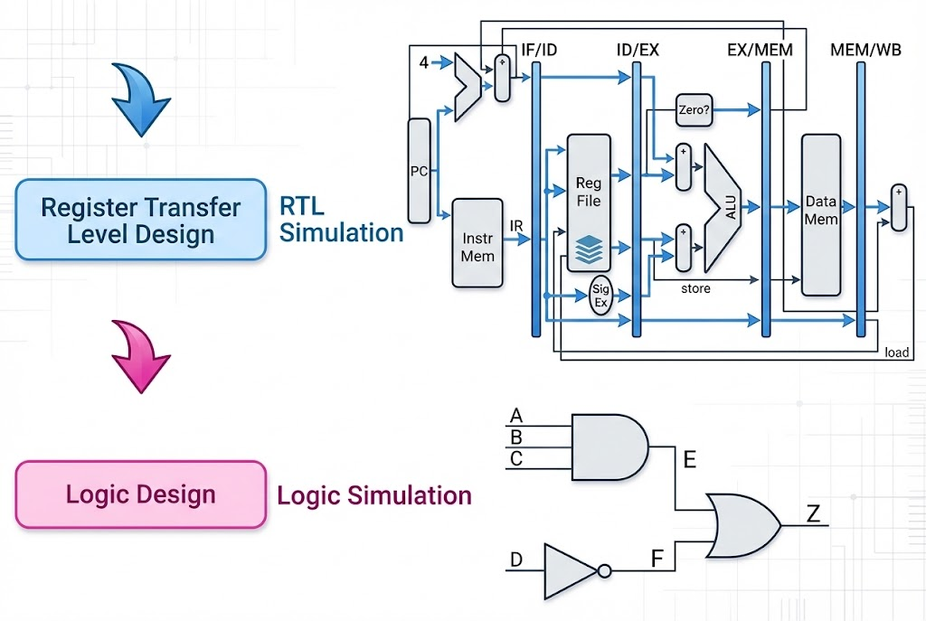
Actual semiconductors contain an enormous number of circuits like the one below.
A huge number of such circuits are incorporated,

To create a functional chip where electrons move on an actual manufactured semiconductor, we must overcome the harsh physical realities of Timing, Power, Noise, Area, and Variation.
This article, 'The Beginning of Implementation (Front-end Bridge)', discusses the stages before and after RTL code is input into the Synthesis Tool.
Verilog coding style: Is it synthesis-compatible code?
The first gateway in the design flow is learning Verilog coding style.
Semiconductor design is extremely complex, costing over $10,000,000 USD to manufacture a chip, with no way to modify it after production. Therefore, "We need hardware coding that is highly reliable and suitable for mass production."

1. Hardware Essence: "It's not code, it's circuits"
Students often mistake Verilog for a programming language like C. However, the ironclad rule for production-ready designs is:
- Understanding Physics: Electrons take time to move (Gate Delay + Net delay). Simulation calculates this as instantaneous ('0' time), but in actual silicon, this time varies with temperature and voltage.
- The Aesthetics of Simplicity: Flashy syntax is only for simulation. Remember that actual chips are just combinations of Combination + Sequential logic.
- Even exceptionally well-made designs can experience Silicon Failure. If you don't make it simple, you won't be able to debug the cause either.
2. Sequential Logic (FF) Design Rules
Flip-flops are the backbone of a chip. Only the most conservative and standard structures are permitted. Of course, even if the promises below are not kept, chip production is actually possible.
However, large companies enforce very strict coding styles to maximize yield even slightly and to enable rapid analysis when silicon failures occur.
- Clock/Reset Conventions:
- Positive Edge Clock: Use only
posedge clkas it is the default in cell libraries. Mixingnegedge clkwithin a single chip is not recommended.(Static Timing Analysis). Mixingposedgeandnegedgecreates 'Half-cycle paths', which halve the timing margin. - If the clock's High and Low durations are not exactly 50:50 (Jitter/Skew), the likelihood of noise issues increases in the mixed
posedgeandnegedgeintervals.
- Positive Edge Clock: Use only
- Asynchronous Reset: Use asynchronous reset, preferably on the
negedge.- Many foundry library cells are optimized for Active-Low asynchronous reset.
- Reliable Initialization: Prefer asynchronous reset to force the chip into a safe 'IDLE' state immediately upon power-up, even before the clock stabilizes.
- No Gating: Do not place logic gates (AND, OR) directly on the clock line; use the ICG as guided by the foundry.
- Glitch Hell: Toggling the clock with a standard
ANDgate can generate short noise pulses. If this enters a flip-flop, it corrupts the data, causing the chip to enter a 'unexplained halt' state. - Foundry-Certified: ICG cells are dedicated components that foundries guarantee are "significantly safer than glitches." Major companies reject designs as 'Lint Errors' if even a single standard logic gate is mixed into the clock line.
- Glitch Hell: Toggling the clock with a standard
Compliant with Standard Syntax: Verilog
always @(posedge clk or negedge rst_n) begin
    if (!rst_n) data_q <= 8'd0; else data_q <= next_data;
end
3. Combinational Logic: wire over reg
This is the most critical point in your submission. You should be cautious about designing combinational circuits using reg within an always @(*) block.
In typical digital circuit design, flip-flops are used instead of latches.
- Risk: Inadequate handling of conditional statements (
if,case) within thealways @(*)block can create unintended latches. While it may work in simulation, it can cause operation to halt at specific temperatures during actual mass production. - Safe Alternative: Preferably use
assignandwirein sequential assignment statements.- Bad (Avoid): Using
assign out = (cond) ? a : b;within analways @(*)block for combinational circuit design (Latch risk) - Good (Safe): Use
assign out = (cond) ? a : b;withassign out = (cond) ? a : b;within analways @(*)block for combinational circuit design (Latch risk) - combined circuit design with
reg- (Latch risk)
- Good (Safe):
assign out = (cond) ? a : b;(Physical circuit clearly visible)
- Bad (Avoid): Using
4. The Essentials of FSM (Finite State Machine) Design
For production-grade FSMs, the key is not 'elaborate case statements' but 'clear signal separation'.
- Separation of State Transitions and Output Logic:
- State Register:
alwaysblock (Sequential) - Next State Logic:
assignstatement (Combinational) - Output Logic:
assignstatement (Combinational)
- State Register:
5. Details to Prevent Mistakes
- Bit Width Matching: Never make the mistake of writing
9'd0when resetting10'd5. The moment you expect tools to roughly compensate, mass production fails. - The Default Value Trap: Abandon the thought of "it probably won't matter." Every
casestatement must have adefault, and everyifstatement must have anelseto ensure all circuit paths are deterministic.
Book Recommendation: Verilog Coding Style for Mass Production
To reiterate, production is possible even without adhering to Verilog coding style. However, large corporations implement these rules to slightly improve yield, slightly reduce the risk of mass production failure, and to make it easier to find the cause if failure occurs. That's why large companies apply these rules.
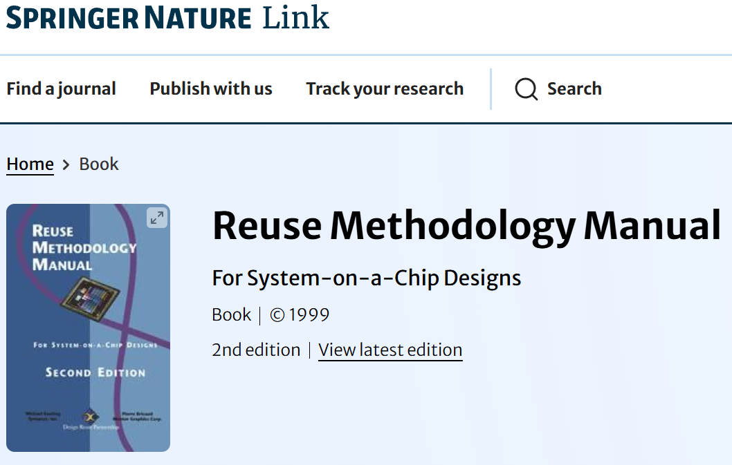
- Reuse Methodology Manual (RMM): The most famous book
- STARC Design Style Guide: I've heard that not only Japanese semiconductor companies, but also engineers from major Korean semiconductor companies who studied in Japan used this book to create many Verilog coding style rules.
- Presentation papers by Verilog expert Cliff Cummings.
Next is RTL Linting. While Lint in software development checks for simple syntax errors or style, Linting in hardware design asks the survival question: "Can this code be converted into an actual circuit?"
Simulators generously accept code that is syntactically valid but impossible to implement in actual hardware, or that causes fatal defects even if implemented. Catching this 'Simulation-Synthesis Mismatch' is the core goal of RTL Lint.1
-Latch Inference: Design Inference and AnalysisEC%9E%90%EC%9D%98-%EC%9C%84%ED%97%98%EC%84%B1">1.1.1 Latch Inference: The Risk of Unintended Memory Devices
One of the taboos in digital circuit design is the creation of 'Inferred Latches'. When describing Combinational Logic, if an if statement or case statement does not explicitly specify the output value for all possible conditions, synthesis tools assume the previous value must be held in situations where the condition is not specified. Since combinational circuits cannot store values themselves, the tool forces the insertion of a Transparent Latch to store the data.
Why Avoid Using Latches?
- Increased Complexity in STA (Static Timing Analysis): Flip-flops transfer data only on the clock edge, making timing analysis straightforward. Conversely, latches have a time borrowing characteristic where clock input changes propagate to the output throughout the transparent window. This makes timing path analysis extremely complex and hinders timing closure by making it difficult for tools to accurately calculate setup/hold times.
- Decreased DFT (Design for Test) coverage: When inserting scan chains for production testing, latches are difficult to control and observe, hindering test pattern generation and reducing fault coverage.
- Glitch Propagation: If a latch's Enable signal is exposed to a glitch, unintended data may be stored, potentially causing functional errors.
Solution: Defensive Coding Style
The most reliable preventive measure is to assign a default value at the very top of every always_comb (SystemVerilog) or always @(*) (Verilog) block. This ensures a default value is assigned even if a specific path is missed in the conditional statement, eliminating the need to maintain the value and thus preventing latch creation.
Example1: Latch created because data_out has no definition when enable is 0
always @(*) begin if (enable) data_out = data_in;
end
Example2: Initialized to 0 upon block entry, so value is determined without entering the if statement -> Synthesized as combinational logic (MUX)
always_comb begin data_out = 1'b0; // Default Assignment if (enable) data_out = data_in;
end
Additionally, when using a case statement, you must include a default clause to prevent undefined states. Without the default clause, the tool attempts to maintain the previous value when an input not matching any case condition arrives, creating a latch.-%ED%95%A8%EC%A0%95-the-evil-twins">1.1.2 Full Case and Parallel Case Pitfalls: "The Evil Twins"
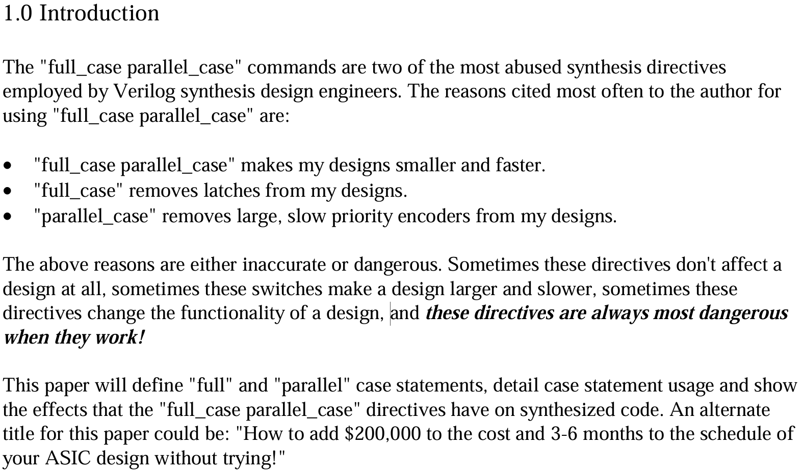
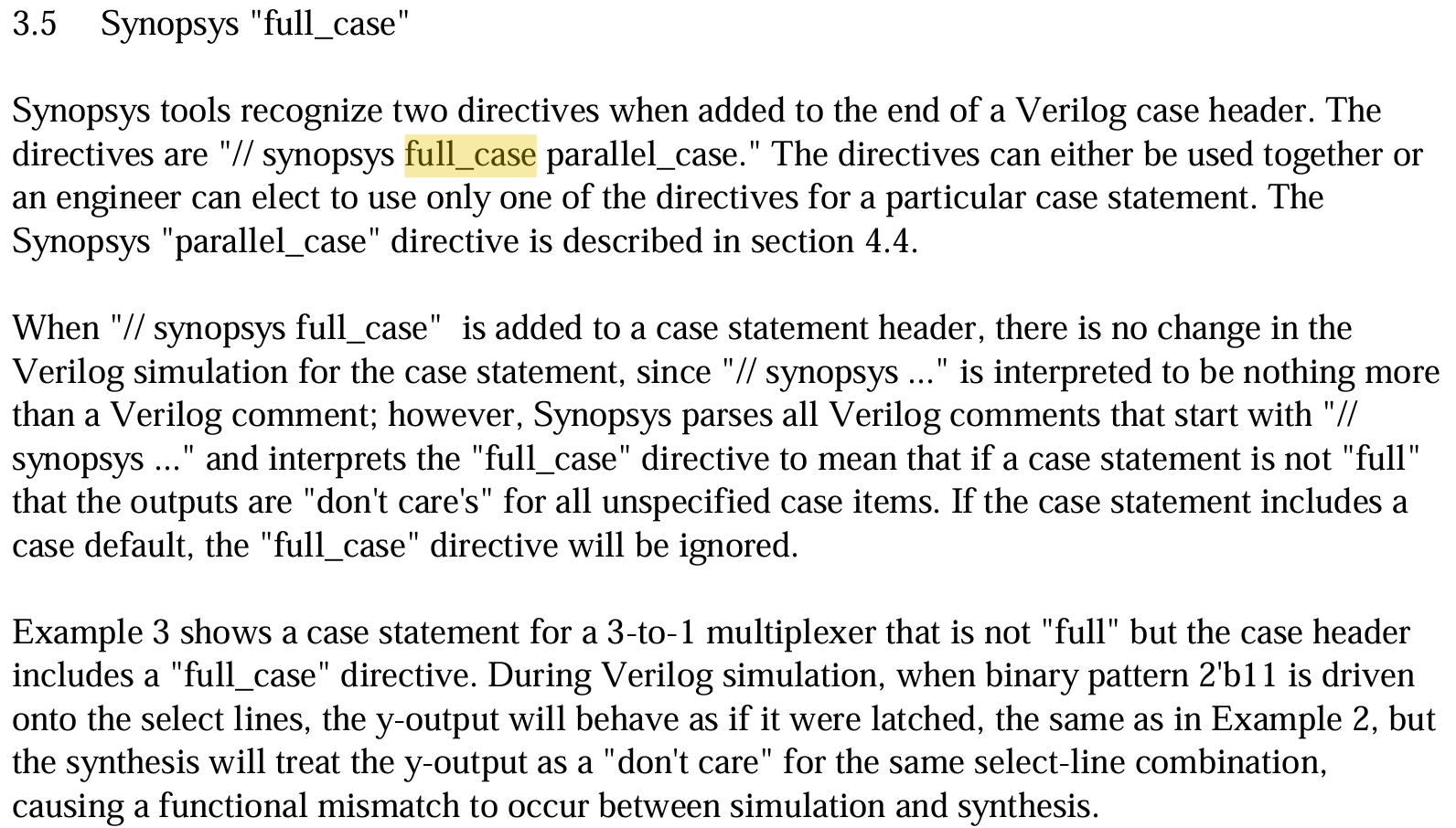
One of the most controversial and dangerous topics in Verilog design history is the use of Sytnehssis Pragma, such as // synopsys full_case parallel_case. Renowned Verilog expert Clifford Cummings dubbed them "The Evil Twins of Verilog Synthesis" and warned of their dangers.
While using these can make your code a bit shorter, it's a style I personally avoid. Just knowing that Synthesis Pragmas exist is sufficient.
Typically, even university labs have small Verilog coding styles.
Startups have them too, and larger companies tend to have stricter Verilog coding styles, along with checkers that enforce these styles.
In the next post, we'll explore RTL Lint.