
Semiconductor Quality Assurance and DFT's Evolution
A7%84%ED%99%94">Semiconductor Quality Assurance and the Evolution of DFT
In the modern semiconductor industry, particularly in System on Chip design, Design for Testability (DFT) has evolved beyond design for post-manufacturing verification. It has become a core engineering discipline that determines the entire product lifecycle and economic viability.

The exponential increase in transistor density driven by Moore's Law has inevitably raised the probability of manufacturing defects. and at the ultra-fine process nodes of 7nm, 5nm, and 3nm, complex defect mechanisms are emerging that cannot be explained by the traditional simple Stuck-at Fault model.
The primary objectives of DFT can be summarized into three main points.
- First is quality assurance through maximizing Fault Coverage. In fields where functional safety is essential, such as automotive, aerospace, and medical devices, it is imperative to maintain DPPM (Defective Parts Per Million) as close to zero as possible.
- Second is reducing test costs. Test time directly impacts chip production costs, so an efficient architecture that detects the maximum number of defects with minimal patterns and time is required.
- Third is yield. Considering defects, such as implementing redundancy designs or enabling on/off control to bypass defective cores. (These are widely used in high-speed CPU designs.)
Scan Architecture: The First Step in DFT.
The challenge in testing digital logic is that it is nearly impossible to externally control and observe the state of a Sequential Circuit containing millions of flip-flops.
Modern semiconductor chips contain hundreds of millions or billions of such circuits. DFT is used to verify that all flip-flops within the chip function correctly, and SCAN design is primarily employed for testing these sequential circuits.
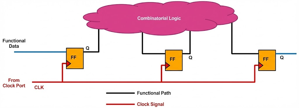
Scan architecture is the most fundamental solution for securing controllability and observability by transforming these sequential circuits into a massive Shift Register in test mode.
2.1 Structure and Operating Principle of the Scan Cell
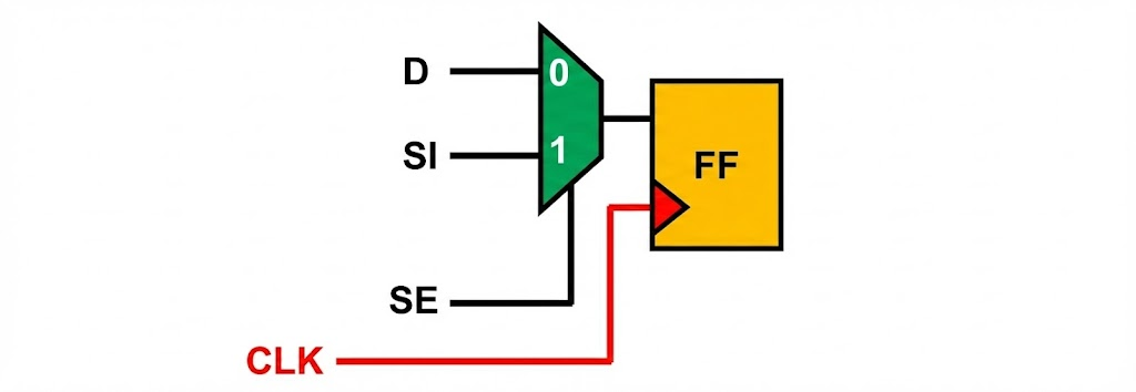
During the RTL synthesis process, the DFT compiler replaces the standard D flip-flops (D-FFs) within the design with specialized cells that incorporate scan functionality. The most widely used industry standard approach is the Mux-D Scan(Multiplexed Scan Flip-Flop) style.
2.1.1 Internal Mechanism of the SCAN D FlipFlop
The Mux-D scan cell includes a functional data input (D), a test-oriented Scan Input (SI), and a Scan Enable (SE) signal to select it. This structure is implemented by adding a 2:1 multiplexer (MUX) at the input stage.
 always @(posedge clk or negedge rst_n) begin if (!rst_n) begin q <= 1'b0; end else begin if (se)
                q <= si; else q <= d; end end
endmodule
- if {SE =0} : The MUX selects the system data input (D) and passes it to the flip-flop. At this time, the chip operates in its original functional mode.
- else: Receives data from SI.
2.1.1 Internal Mechanism of the SCAN D FlipFlop
This substitution process occurs automatically in the netlist, and the added MUX may introduce a slight delay in the data path. Therefore, DFT engineers must update the Timing Constraints after SCAN Insertion and analyze the impact on the timing margins (Setup/Hold margin) of the functional path.
Looking back at our circuit, it now appears as follows.
2.2 SCAN Insertion
Synthesis Tool For example, in DesignCompiler, using compile -scan, it changes it to a SCAN Cell. The synthesis tool only changes the Cell.
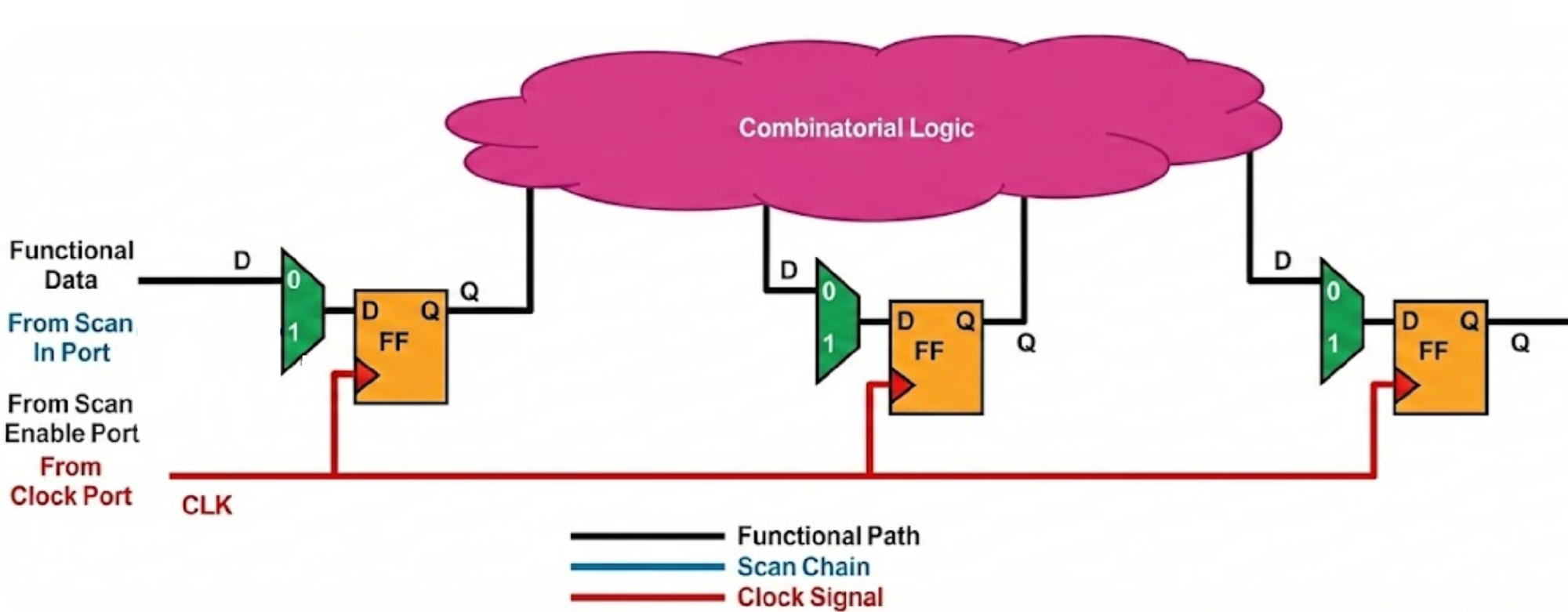
2.2 Scan Stitching and Chain Optimization
Once the scan cells are substituted, the DFT tool performs the stitching process to connect them. Configuring millions of flip-flops into a single chain would cause test time to increase exponentially, so in actual implementation, it is divided into multiple parallel scan chains.
The key is:
- SCAN Shift mode: When Scan Enable is 0, the function mode operation of the base RTL
- SCAN Capture mode: When Scan Enable is 1, the Signal at the Scan In Port bypasses Combinational Logic and only undergoes Signal shifting through the Scan Flip-Flops.
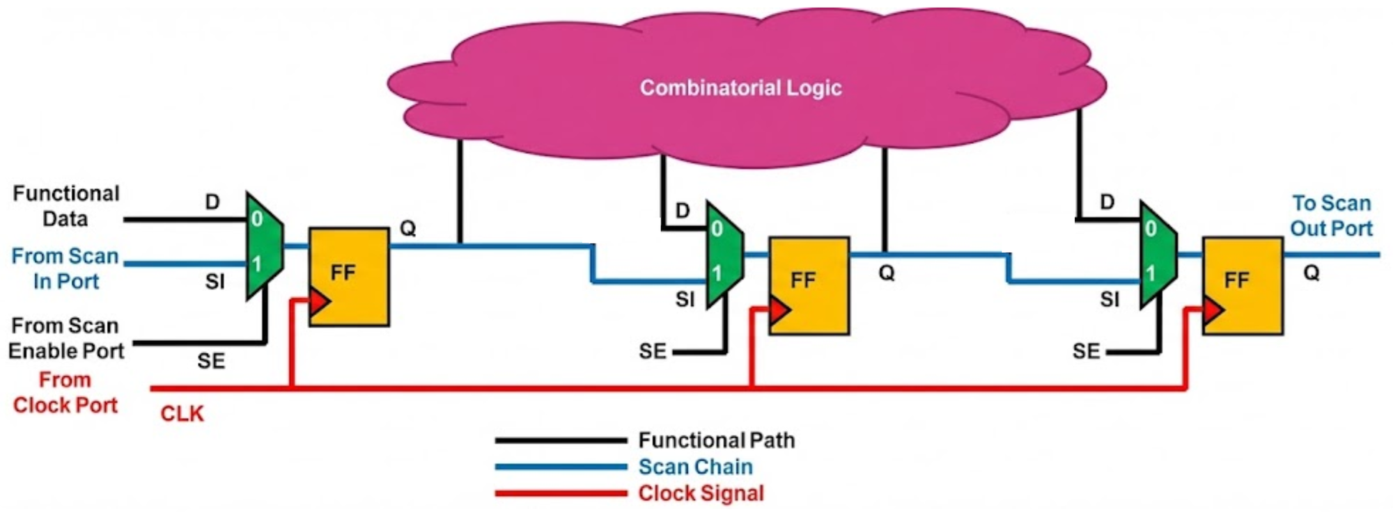
2.2.1 Scan Chain Input Output Budgetting
To optimize the ATE's memory efficiency and test time, it is important to balance the length of all scan chains. This is called Chain balancing. For example, if there are 10,000 flip-flops total and 100 scan channels are available, each chain consists of 100 flip-flops.
If length imbalances occur between chains, shorter chains must wait until the longest chain completes its shift, resulting in unnecessary padding data and wasted test time.
Foundries share recommended SCAN I/O budgeting tables by flip-flop count, considering these factors.
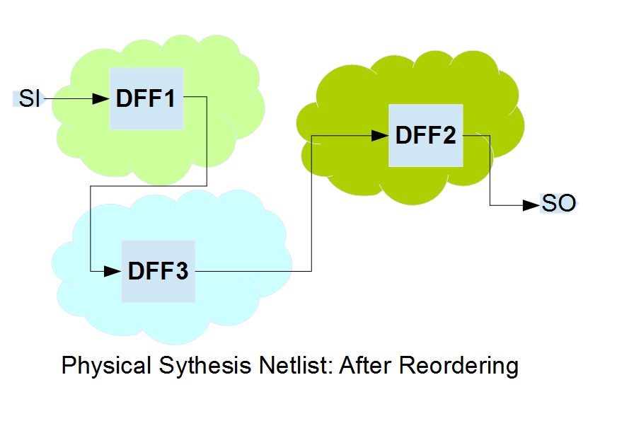
2.2.2 SCAN Chain Reordering
The SCAN chain stitching step does not consider the geometric coordinates of the cells. This can cause severe routing congestion during the Place & Route phase. Physically distant cells connected adjacent on the chain result in long traces spanning the entire chip.2026/01/image-67.png" class="kg-image" alt="" loading="lazy" width="928" height="241" srcset="https://www.vlsi.kr/content/images/size/w600/2026/01/image-67.png 600w, https://www.vlsi.kr/content/images/2026/01/image-67.png 928w" sizes="(min-width: 720px) 720px">
https://vlsibasic.blogspot.com/2014/09/scan-chain-reordering.html
After P&R:
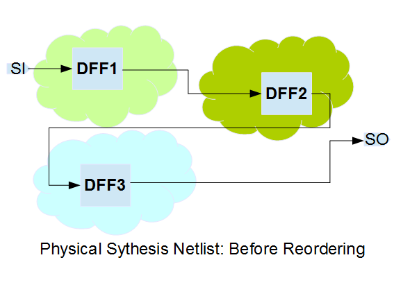
To address this, the P&R tool performs Scan Reordering. After the physical placement of cells is finalized, the tool dynamically changes the connection order of the scan chain by finding a path that minimizes wiring length. This is an essential process for securing timing margins and reducing chip area.
After Scan Reordering:
2.3 Lockup Latch: Clock Skew Management and Hold Time Violation PreventionEB%B0%A9%EC%A7%80">2.3 Lockup Latch: Managing Clock Skew and Preventing Hold Time Violations
In large-scale SoCs, scan chains frequently cross different clock domains or must travel extremely long physical distances even within a single clock domain. The resulting clock skew can cause critical hold timing violations during shift operations.
2.3.1 Hold Violation:
- Suppose the clock for the launch flip-flop sending data within the scan chain arrives later than the clock for the capture flip-flop.
- When the launch flip-flop outputs new data, the capture flip-flop may still not have captured the previous data.li>
- A hold time violation occurs.
2.3.2 Function and Placement of the Lockup Latch
To resolve these issues, the lockup latch is placed at clock domain transition points or locations with significant skew.EB%B0%B0%EC%B9%98">2.3.2 Role and Placement of Lockup Latches
To resolve these issues, Lockup Latches are inserted at clock domain transition points or in sections with significant skew.
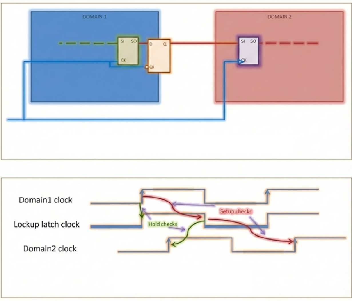
- Place a Lockup latch at the end of Domain1. The key point here is to use a Negative Lockup latch, which operates on the opposite clock phase to the Flipflop.
- At the end of Domain1, when the Clock Level transitions from 0 to 1 (rising edge), the Data does not propagate to Domain2 but only propagates up to Lockup D.
- Only when the clock transitions to the low level does the lockup latch propagate the data to Domain2.
Consequently, the data arrives at Domain2 delayed by half a clock cycle.
This ultimately facilitates meeting the hold time requirement.
3. ATPG (Automatic Test Pattern Generation): The Engine for Fault Detection
Once structural tests for the design are prepared, "test input patterns and corresponding output vectors" must be generated to detect actual faults.
For example, "When the cola button on a vending machine is pressed, cola should be dispensed. If not, it's a fault." This is a test pattern.
3.1 Advancement of Fault Models
As process technology advances, the nature of faults changes, so the methods for modeling them have also evolved.
3.1.1 Stuck-at Fault
This is the most classical and widely used model. It assumes that routing is interrupted midway or stuck to VDD, causing a specific circuit node to be permanently fixed at logic value '0' (Stuck-at-0) or '1' (Stuck-at-1).
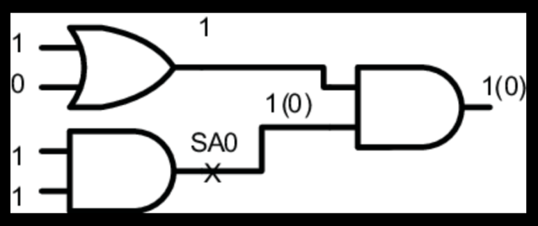
- Testing Method: For example, to detect a Stuck-at-0 defect in the output of an AND gate, apply an input pattern that can make the output '1' and observe whether the output matches the expected value.
- Limitations: Can only detect static(Static) defects and cannot detect timing-related defects.
Creating these test patterns is the role of ATPG.
Searching for ATPG algorithms like D-Algorithm or PODEM will yield extensive resources on digital engineering.
3.1.2 Transition Fault and Delay Fault
Although the routing is not broken, if the routing is processed too thickly or too thinly, the RC value of the net changes, causing a phenomenon where the speed varies.
- Slow-to-Rise: The time taken to transition from 0 to 1 is too long.
- Slow-to-Fall: The time taken to transition from 1 to 0 is too long.
- Path Delay Fault: Tests the cumulative delay of the entire path within the circuit, not the delay of individual gates.
3.2 At-Speed Test and Clocking
To detect delay faults, an At-Speed test driving the chip at its actual Chip function frequency is essential. However, externally applied clock frequencies are typically very slow.
This requires IP such as an On-Chip Clock Controller.
3.3 Test Compression
As chip sizes increased, scan chains grew longer, and the number of patterns for At-Speed testing increased, leading to an explosive rise in test data volume and test time. To address this, scan compression technology was introduced.-embedded-deterministic-test">3.3.1 Compressor, MISR, and Embedded Deterministic Test
Compressor is a technology from Synopsys, while EDT is a technology popularized by Mentor (now Siemens EDA). Both perform compression by adding hardware logic inside the chip.
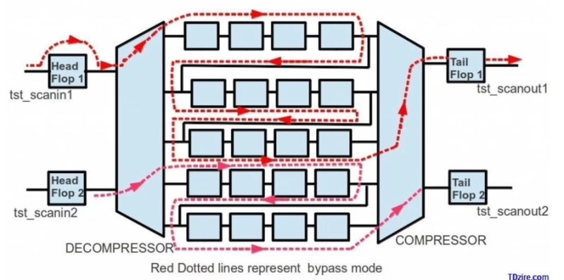
- Decompressor: Located at the chip's input, it receives data compressed into a small number of channels from the ATE and broadcasts it to numerous short scan chains within the chip. It supplies low-correlation random patterns using a Ring Generator and Phase Shifter.
- Compactor: Located at the output of the scan chains, it compresses the results of numerous internal chains into a small number of channels via an XOR tree or Spatial Compactor and sends them to the ATE.
- X-Masking: To prevent uninitialized values(Unknown 'X') contaminating the compressed Signature. This logic is essential to mask the X values.
- MISR: Instead of comparing outputs every cycle, it uses a Multiple Input Signature Register to accumulate the results of the entire pattern into a single Signature, then compares it only once at the end of the test.
As seen, SCAN is a design domain. ATPG is a test domain that can be performed even after tape-out.
And as you can see, while the actual operation matching the chip's purpose is crucial, testing incurs enormous costs (complex design, additional area and ports for testing).
For example, SCAN Shift generates extremely high signal switching activity, leading to massive power consumption, heat generation, and even HCI, BTI, IR, and EM issues. Therefore, the DFT field is quite diverse in its research topics.
4. MBIST (Memory Built-In Self-Test)
Memory, which occupies nearly half the area of modern SoCs, has a much higher transistor density than logic and is therefore more vulnerable to manufacturing defects.
Scan tests are optimized for testing flip-flops and logic gates, making them unsuitable for detecting minute capacitive defects within memory cells or interference between adjacent cells. Therefore, the MBIST dedicated memory test engine is essential.
4.1 March Algorithm
The MBIST controller is embedded within the chip itself, enabling it to write and read data to the memory and verify its operation without the need for external equipment. The standard algorithm used for this is the March Algorithm. The March Algorithm sequentially marches through the memory address space, performing a series of read/write operations.
4.2 Built-In Self-Repair, BISR
Memory is a major cause of yield degradation, so discarding an entire chip due to a detected defect represents significant economic loss. To prevent this, BISR technology is applied.
- Redundancy: During memory design, redundancy rows and columns are pre-allocated.
- Repair Process: If a defective cell is found during MBIST testing, the controller stores the corresponding address information. After the test, this information is permanently recorded in the chip's internal eFuse (Electrical Fuse).
- Remapping: When the chip boots, the HW Logic reads the fuse information and physically remaps the defective addresses to spare rows/columns. This process is invisible to the user, and the chip operates normally as if it were defect-free.
5. LBIST (Logic Built-In Self-Test)
LBIST is a technology enabling logic circuits to self-test, allowing chips to detect defects without ATE. This is crucial not only during chip manufacturing but also also plays a crucial role in complying with the ISO 26262 functional safety standard, which requires verifying chip integrity during power-on (Power-On Self-Test) or operation (Run-Time Test).
5.1 STUMPS Architecture and Components
LBIST is implemented based on the STUMPS (Self-Test Using MISR and Parallel Shift register sequence generator) architecture.
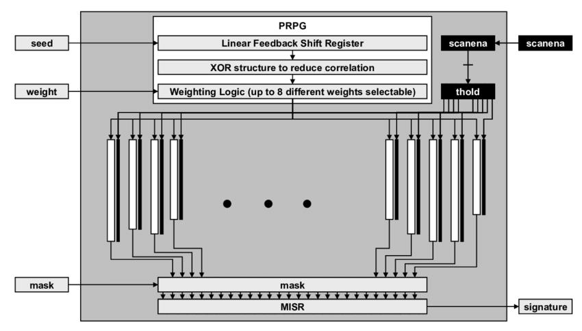
- PRPG (Pseudo-Random Pattern Generator): Instead of using stored patterns like ATPG, it uses a LFSR (Linear Feedback Shift Register) to generate pseudo-random patterns every cycle. This enables the generation of very large patterns without requiring additional memory.
- Phase Shifter: The output of the LFSR may exhibit structural dependencies. The phase shifter mixes this through an XOR network, eliminating the correlation of data entering adjacent scan chains and increasing the randomness of the pattern.
- MISR (Multiple Input Signature Register): Since outputs from thousands of scan chains cannot be stored, they are compressed and converted into fixed-length signatures. This is analogous to the inverse structure of an LFSR performing polynomial division operations.
5.2 Golden Signature and X-Pounding Problem
LBIST verification is performed by comparing the final signature generated after test completion with the Golden Signature pre-calculated through simulation. If the two values match, it passes; if even one differs, it fails.
The biggest challenge in this process is handling the 'X' (Unknown) value. Uninitialized memory within the circuit, outputs from analog blocks, or floating nodes appear as 'X' in simulations.
While ATPG can ignore this, LBIST's MISR corrupts the entire Signature the moment this 'X' value enters, turning it into an unpredictable value. To prevent this, either eliminate the cause of 'X' during the design phase or add X-Blocking logic to block the path to the MISR.
6. Standard Interfaces: Connecting the Chip to the Outside World
A SoC is a complex system composed of numerous IP cores (CPU, GPU, DSP, Memory Controller, etc.). Internationally standardized interfaces are used to control and test these components individually.
The IEEE1149, 1500, and 1687 are frequently used, and in the 3D-IC era, 1838 will likely be widely adopted as well.
Conclusion: Future Outlook for DFT Technology
As we have seen, DFT is not merely an add-on feature in semiconductor design but a core architecture responsible for chip yield, cost, quality, and safety.
Future DFT technology is expected to evolve in the following directions.
- AI-based DFT & ATPG
- 3D-IC, HBM, and chiplet testing
- High-Speed I/O Loopback Test:
In conclusion, as processes become finer and chips more complex, the importance of DFT will only grow. The 'DFT-First' methodology, which considers DFT from the earliest design stages, will become an essential requirement for semiconductor success.