
1. The Shift in the Tapeout Paradigm and the Evolution of Physical Verification
Semiconductor integrated circuit design has been a relentless battle against increasing complexity for decades. Starting with a few dozen transistors, early integrated circuits have now entered the realm of Angstrom-scale processes at 7nm, 5nm, 3nm, and below, evolving into massive systems integrating tens of billions of transistors on a single die.
Physical Verification, performed immediately before Tapeout—the final gate in the RTL-to-GDS flow, performed just before the final gate of tapeout, is the stage that exerts the greatest psychological and technical pressure on engineers. A single minute design rule violation or layout versus schematic mismatch can result in mask cost losses amounting to billions of won and cause a fatal silicon respin, leading to a missed market entry window.
Therefore, modern Physical Verification engineers must possess convergent knowledge that extends beyond simple EDA tool operation, encompassing semiconductor device physics, the optical characteristics of Lithography processes, the mechanical dynamics of CMP (Chemical Mechanical Polishing) processes, and circuit theory.
2. Fundamentals of Data Integrity and Verification: PDK and Sign-off Criteria
2. Fundamentals of Data Integrity and Verification: PDK and Sign-off Criteria2.1 Definition of Sign-off and Foundry Contracts
In the semiconductor design flow, 'Sign-off' refers to the formal approval process confirming that design data meets all technical and quality requirements for manufacturability and operational assurance before being transferred to the foundry for production. Physical Verification Sign-off, together with Timing Sign-off, determines the success of the chip. to ensure manufacturability and functional integrity. Physical Verification Sign-off, together with Timing Sign-off, forms the critical sign-off axis determining the chip's success.
Upon successful completion of Physical Verification, the design data undergoes a Stream-out process. It is converted into the GDS (Graphic Data System) or OASIS(Open Artwork System Interchange Standard) format and delivered to the foundry. (OASIS format is primarily used recently.)
At this moment, the outcome of Physical Verification serves as a guarantee that the designer has fully complied with the Design Rule Manual (DRM), the 'Lithographic Contract' provided by the foundry. The foundry fabricates masks based on this data. Should yield degradation occur due to unvalidated violations, responsibility lies entirely with the design side. Therefore, the sign-off criteria function as an absolute baseline that cannot be compromised.
2.2 PDK: The Constitution of Physical Verification
All standards for Physical Verification are defined within the Process Design Kit (PDK) provided by the foundry. The PDK is not merely a collection of files; it is a core asset that quantifies the foundry's process capabilities and limitations. The PDK contains a Rule Deck (Runset) for Verification Checks, which consists of code performing inspections such as DRC, LVS, and ERC.
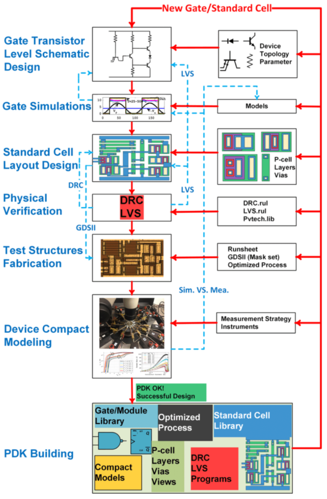
The PDK contains the Primitive Device Library, Symbols, and P-Cell (Parameterized Cell) information. From a verification perspective, the most critical files are the Rule deck and Run set File. These files are written according to the syntax of the EDA tools used (Calibre, Pegasus, IC Validator, etc.) and are updated based on the foundry PDK version.
Engineers must verify the PDK version early in the project and ensure that the latest Design Rule Manual (DRM) changes are reflected in the current Rule Deck. Particularly in leading-edge processes, where process maturity is low and rule changes are frequent,, it is essential to track and manage the foundry's latest rule patches right up until tapeout.-%ED%8F%AC%EB%A7%B7%EC%9D%98-%EC%A7%84%ED%99%94-gdsii%EC%97%90%EC%84%9C-oasis%EB%A1%9C">2.3 Evolution of Layout Data Formats: From GDSII to OASIS
Traditionally, layout data was stored in the GDS format, followed by the GDSII format. Semiconductor design data is enormously large, and the means to store such data was enormous tape. sending this data from fabless companies to foundries was called "tape-out." The foundry used this data in the lithography process after undergoing the MDP (Master Design Process).

However, as chip complexity increased, the size of GDSII files exploded from tens of gigabytes to terabytes. This has become a major cause of delays in data transfer times and EDA tool loading times. OASIS provides compression ratios 10 to 50 times higher than GDSII and supports 64-bit precision, enabling efficient representation of complex geometries in ultra-fine processes.
Caution is also required regarding potential data loss or Grid Snapping Errors during the conversion process between GDSII and OASIS formats. This can lead to major issues.p>
Errors can also occur due to layer map mismatches when merging Blackbox data or Hard Macros received from IP vendors with the Top-level design. This can lead to unintended layer-to-layer checks during verification or the disappearance of shapes that should exist, resulting in critical failures. Strict data management protocols are therefore required.
3. Design Rule Check (DRC): Geometric Compliance for Manufacturability
Design Rule Check (DRC) is the most fundamental step in Physical Verification. It involves a comprehensive inspection to ensure all geometric shapes in the layout satisfy the physical constraints defined by the foundry. This process fundamentally answers the question: "Can this design be physically manufactured?" and reflects the limitations of the lithography process and the characteristics of the etching process.
Semiconductor circuits are drawn as follows: The circuit diagram is drawn on a mask, and light is used to etch it onto the wafer.p>

3.1 Basic Mechanism of DRC and Boolean Operations
Traditional DRC performs one-dimensional distance measurements and two-dimensional area calculations for each layer in the layout. These checks create derived layers based on Boolean operations (AND, OR, NOT, XOR, etc.) between layersto generate derived layers, which are then measured.
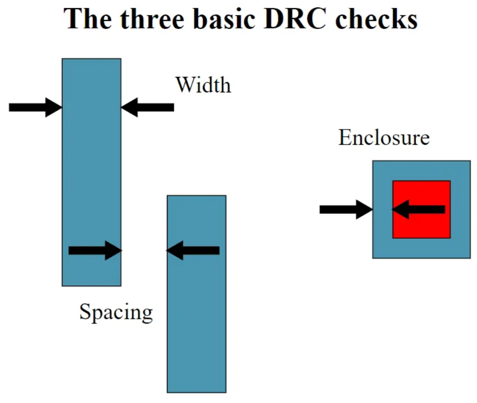
- Width Check specifies a minimum width to prevent Open defects caused by patterns breaking during processing due to excessive thinness, or to prevent electrical performance degradation from resistance values exceeding the allowable range.
- Space Check prevents Short defects caused by adjacent patterns sticking together due to light scattering during lithography when their spacing is too narrow.
- Enclosure Check inspects the clearance around Vias or Contacts to ensure Metal pads do not extend beyond the upper/lower Metal pad area, preventing connection failures.
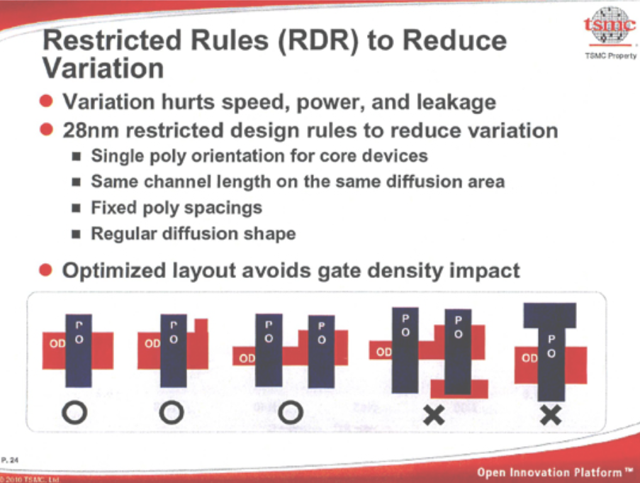
3.2 Advanced Node DRC: FinFET and RDR
With the introduction of sub-20nm processes, particularly FinFET technology, DRC rules have evolved beyond simple geometric constraints into a highly stringent and complex form known as RDR (Restricted Design Rules). This is due to the physical limitations of patterning features much smaller than the wavelength of light (193nm).
3.2.1 Multi-Patterning and Coloring Conflict
Forming features below 10nm in a single exposure using 193nm ArF immersion lithography equipment has become physically impossible. To overcome this, the industry has introduced Double Patterning (DPT) or Multi-Patterning (MPT) technology. This involves sequentially exposing a single layer (e.g., Metal 1) using two or more masks(Decomposition) sequentially to reduce pitch.
- Problem Summary: The pen we use (light source: ArF, 193nm) is too thick, while the lines (patterns) we need to draw are too thin, at the 10nm level.
- Symptom: Drawing lines too close together causes them to blur together due to light diffraction (resolution limit).
- Solution: Since we cannot draw everything at once, let's divide the drawing into two (DPT) or more (MPT) steps.
Solution: Coloring, Double patterning
- Definition: The process of splitting one layer into two masks (Mask A, Mask B).
- Analogy: Drawing once with a 'red pen', then drawing again with a 'blue pen'.
- Rule: Patterns with narrow gaps must be drawn in a different color.
Coloring Methodology: LELE vs SADP
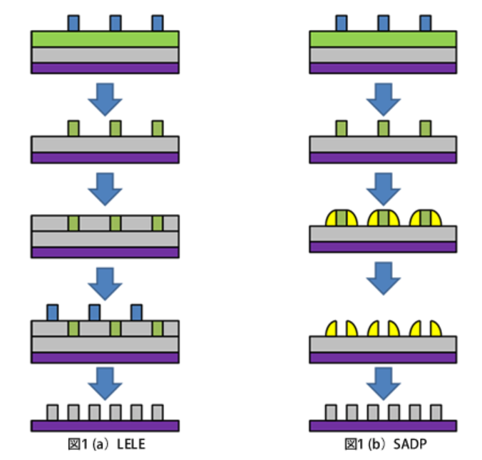
- LELE (Litho-Etch-Litho-Etch): A method using two masks and two bakes.
- Disadvantages: The overlay between the two masks must be perfectly aligned.
- SADP (Self-Aligned Double Patterning): Uses only one mask, creating patterns by erecting spacers around a mandrel.
- Advantages: Physically erects walls, eliminating alignment errors (self-aligned).
- Characteristics: Requires complex algorithms to determine if a structure can support walls, not just simple distance-based DRC.li>
3.2.2 FinFET/GAA Specific Rules: Grid, Quantization
Unlike conventional planar transistors, FinFET devices have a 3D structure. The channel width is quantized based on the number of fins, not a continuous value. This imposes strict regularity requirements, limiting design flexibility.
Fin Grid means all fins must be precisely placed on a predefined grid. DRC tools strictly check for Off-grid states where fins deviate slightly from the specified grid.
Furthermore, In FinFET processes, the Cut Mask step is essential. This involves forming long Poly-Silicon Gates or Metal Routes and then cutting away the unnecessary portions. The positioning accuracy of the Cut Mask, the End-to-End Spacing between Cuts, and the impact of Cuts on surrounding patterns are critical to yield, making verification extremely challenging. Particularly, the complex interconnect structures in the Middle-Of-Line (MOL) layer often become the primary cause of numerous DRC violations.
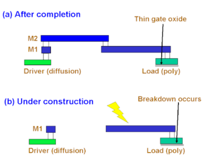
3.3 Antenna Effect
- Cause: During the Plasma Etching process, ionized charges accumulate on the Metal.
- Symptom: The Metal acts like an antenna, collecting charges. If these charges have no outlet, they pass through the Gate Oxide (Fowler-Nordheim Tunneling).
- Result: Permanent damage to the transistor or Vth fluctuation occurs.
3.3.1 Antenna Ratio Calculation (Calculation)
Semiconductor design tools (DRC) use the Antenna Ratio as a key parameter.EC%82%B0-calculation">3.3.1 Antenna Ratio Calculation
Semiconductor design tools (DRC) monitor whether the Antenna Ratio exceeds the threshold value.
- Basic Formula: Antenna ratio = Total Metal area / Gate Oxide Area
- Cumulative Check: Process layers are stacked from the bottom up. Therefore, sum the area of all connected metal/vias from Metal 1 up to the current process layer.
- Side-wall Area: As processes become finer, wiring becomes thinner and taller. Now, charge entering not only through the top surface but also through the side walls(Thickness) can no longer be ignored and is included in the calculation.
3.3.3 Solutions
Engineers prioritize Jumper solutions and use Diode (Antenna cell) as a last resort.
① Jumper Insertion (Metal Hopping)
- Principle: This method involves breaking a long wiring path midway, temporarily routing it to an upper layer, and then routing it back down.
- Why does it work? The process flows from bottom to top. When etching the lower layer, the jumper keeps the length of the wiring connected to the Gate physically short. The entire wiring is connected only after the lower layer's protective layer is already formed.
- Advantage: This solution minimizes power issues.
② Diode Insertion
- Principle: A diode is placed near the Gate to create a lightning rod, allowing charge to escape to the Substrate.
- Advantages: Provides a simple solution when complex routing leaves no space for jumpers.
- Disadvantages: Generates leakage current.
3.4 Density Check and Planarization Algorithms
- CMP (Chemical Mechanical Polishing): A process that flattens the wafer surface by rubbing it with a chemical solution and a mechanical pad.
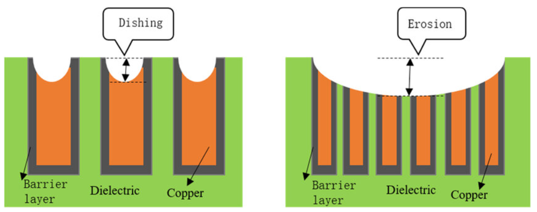
- Issues: Areas with more metal (Hard) and areas with only insulator (Soft) have different etching rates.
- Dishing: Soft areas become locally etched deeper.
- Erosion: Hard areas cause surrounding material to be etched away as well.
- Result: A bumpy surface causes misalignment when depositing the next layer (poor DOF), and the varying metal thickness leads to unexpected resistance values.
3.4.1 Density Check Methodology: Sliding Window
It is too computationally intensive for a computer to inspect the entire chip at once. Therefore, it inspects by examining small 'windows' sequentially.
- Window & Step Size: For example, it checks a 1m window by sliding it 1cm at a time to the side.
- Density Range: A rule is applied: "This window must contain metal covering at least 20% to a maximum of 80% of its area."
- Gradient Check: It also checks that the density doesn't suddenly change drastically compared to the adjacent window.
3.4.2. Solution: Dummy Fill
We force Dummy Metal into low-density empty spaces to balance the density.
Various methodologies exist, such as Simple Fill and Smart Fill. Simple Fill, for instance, it simply places square dummy fills in a grid pattern within the empty space. The key point to remember is that density maintenance is necessary to "ensure all cells at every coordinate have the same properties," and that fillers are inserted into empty spaces.
4.1 Core Algorithm of LVS: Hidden Picture Search (Graph Isomorphism)
LVS verification is the process of solving the Graph Isomorphism problem, which mathematically compares whether two graphs are structurally identical. The tool primarily undergoes two stages.
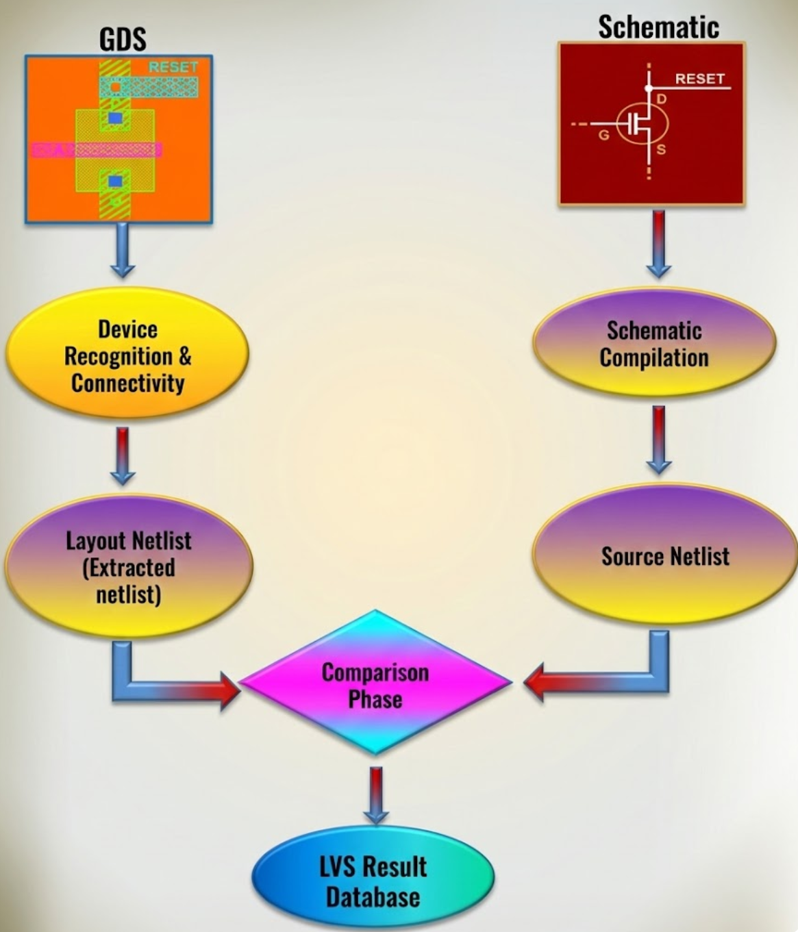
- Extraction: This step involves the tool scanning the complex shapes drawn on the layout and recognizing them as "this is a transistor, this is a wire." For example, When Poly and Active layers overlap, it recognizes them as a MOSFET. When Metal and Via overlap, it groups them into a single electrical path called a 'Net'. This process converts the graphical data into electrical information, the 'Layout Netlist'.
- Comparison: The schematic drawn by the designer and the newly extracted layout are each converted into graph models. Components become nodes, and wiring becomes edges. The LVS engine compares whether the connectivity patterns of these two graphs match topologically 100%.
4.2 Simple Linking and Beyond-Connection-Parameter-Comparison">4.2 Beyond Simple Connectivity: Parameter Verification
Matching the graph's connectivity isn't the end of the story. LVS acts like a meticulous construction supervisor. It doesn't just check if "the room and living room are connected," but also verifies if "the width of that door precisely matches the design drawing."
- Device Parameters: The transistor's W(Width), L(Length), resistance values, capacitance sizes, etc., must match the schematic values and the physical dimensions on the layout within tolerance limits.
- Multiplier & Fingers: Verifies whether a device set as
m=2in the schematic is actually drawn as two separate devices on the layout, or if it was merged into one large device. - Initial Correspondence: Since it is impossible to randomly compare tens of thousands of devices, the LVS tool uses text (Label/Pin) names or the unique connection structure of a specific device as an 'Anchor' to start the comparison. Therefore, it is extremely important to enter the Port Text accurately.
4.3 Major LVS Error Types
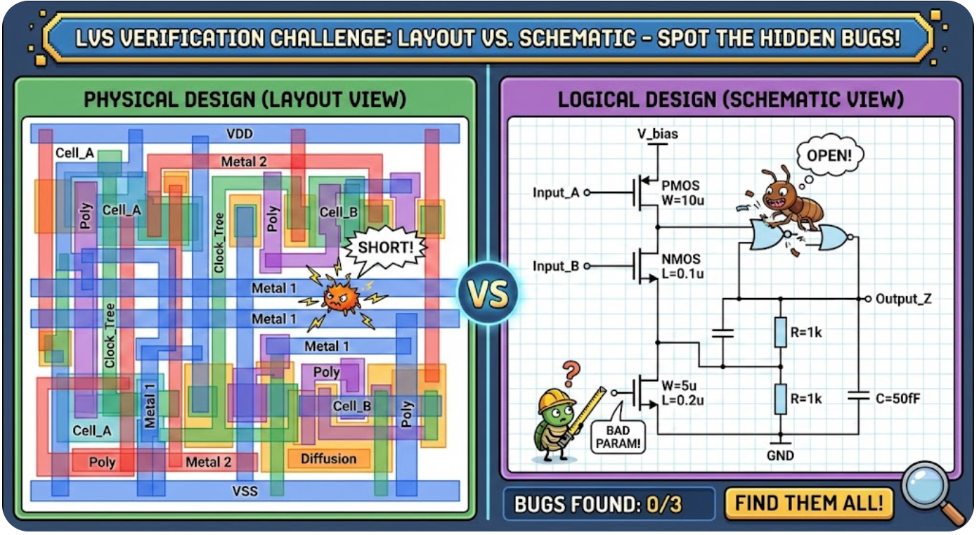
1) Short
"The most common, yet most critical error"
This occurs when two distinct signal lines physically touch each other on the layout.
- Symptom: Net A and Net B, which are separated in the Schematic, are connected in the Layout.
- Cause: This can be caused by slight overlap of Metal due to insufficient routing space or a misplaced Via.
- Characteristics: When a Short occurs, the graph structure is completely destroyed, so a single Short can trigger hundreds of False Errors. Always address shorts first.
2) Open
"When a connection should be present but is missing"
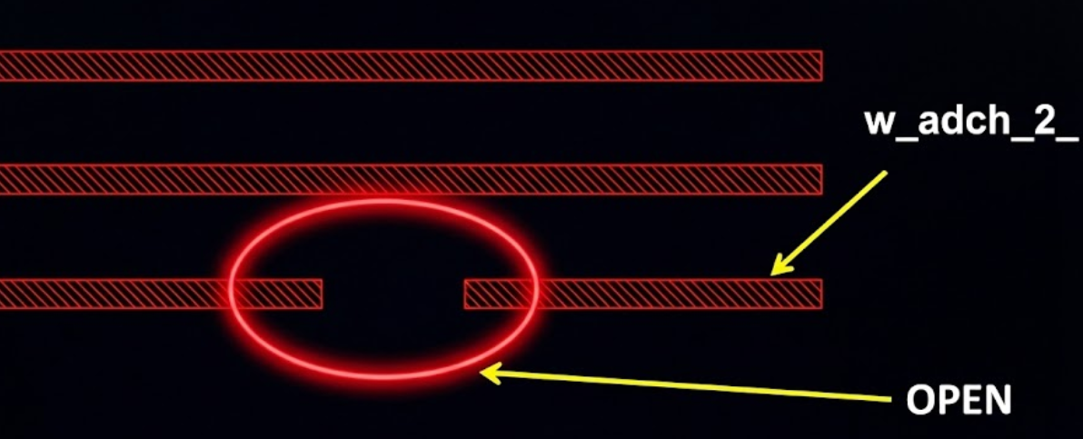
This occurs when a section that should be connected as a single Net is broken.
- Symptom: In the schematic, it is Net A, but in the layout, it is recognized as split into Net A_1 and Net A_2.
- Cause: Often occurs when a long trace has a broken metal layer or a via connecting layers is missing.
- Soft-connect: A warning may also appear when connections are only made to high-resistance layers (e.g., N-well, Substrate) without metal connections.
3) Device Mismatch
This occurs when the structure is correct, but the 'specifications' are wrong.
- Parameter Mismatch: When the W/L size is different or the number of fingers is different.
- Device Type Mismatch: When
nmos_lvt(Low threshold) should be used, but a standardnmosis used instead. This often occurs due to incorrect process mask definitions leading to incorrect device recognition.
5. ERC (Electrical Rule Check)
If DRC checks "Is the drawing correct?" and LVS checks "Are the connections as per the design?", ERC checks "Is this chip electrically safe and robust?". Even if the connections are correct, it's useless if it burns out the moment power is applied. ERC is the process of finding a semiconductor's electrical vulnerabilities.
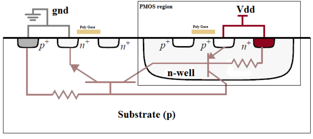
This is usually not a problem, but if large noise or overvoltage spikes occur externally, these devices suddenly wake up and trigger each other (Thyristor), shorting the power supply (VDD) and ground(VSS). This causes excessive current to flow, causing the chip to burn out. This is called Latch-up.
- Geometric Inspection: This rule states, "It's dangerous, so densely place 'Well Taps' on the board." Measure the distance between transistors and Taps; if it's too far, it's a Violation.
- Topology-aware Check: It doesn't just measure distance; it also considers "Which is more vulnerable?" For example, components directly connected to external pins (I/O pads) are more exposed to external impacts, right? It rigorously checks whether stronger protective barriers (Guard Rings) are placed around these 'high-risk' components.B2%BC%EB%9D%BD%EC%9D%84-%ED%94%BC%ED%95%98%EB%8A%94-%ED%94%BC%EB%A2%B0%EC%B9%A8-%EC%84%A4%EA%B3%84">5.2 ESD (Electrostatic Discharge): Lightning Rod Design to Avoid Lightning
Electrostatic discharge (ESD) is like lightning for semiconductors. If static electricity 'zaps!' during manufacturing or use, the chip's internal circuits melt. That's why chips have protective circuits (lightning rods) that safely ground static electricity. These are called clamp cells, and ERC verifies they function properly.
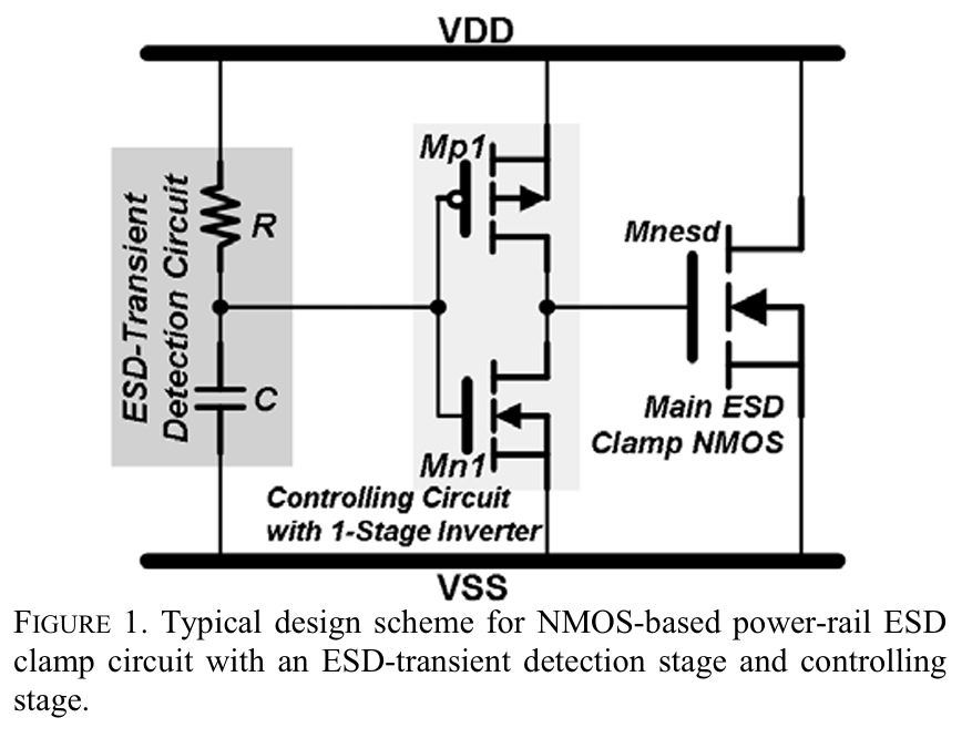
- P2P (Point-to-Point) Resistance Test: The path from the external pin to the protective device must be wide open like a 'highway'. If the resistance of this metal wiring is high (if the path is narrow), the static electricity cannot escape in time and overflows into the internal circuit, destroying the chip.
- CD (Current Density) Test: We examine the 'thickness' of the metal. When an enormous current like static electricity flows, if the wiring is too thin, it cannot withstand the heat (Joule Heating) and the wiring itself melts and breaks. It's like a water pipe bursting under water pressure.
Additionally, we verify that there are no issues with power intent, such as level shifters.