
The modern semiconductor industry continues to push beyond the limits of transistor integration predicted by Moore's Law. This is the VLSI era, where billions of transistors are integrated onto a silicon die the size of a fingernail.Physical Design, commonly known as Place and Route (P&R), which converts RTL code into a GDS file—a physically manufacturable layout—has evolved beyond simple Code-to-Code automation. It now represents an extreme multi-variable optimization problem.
Whereas P&R in past µm-scale processes was a simple geometric puzzle of placing devices and connecting lines, P&R in 7nm, 5nm, and 3nm and below FinFET and Gate-All-Around processes represent the pinnacle of complex physical engineering, requiring consideration of quantum effects, electromagnetic interactions, and the physical limits of the manufacturing process itself.
P&R is an NP-Problem with an overwhelming number of possible cases.
1. Design Partitioning
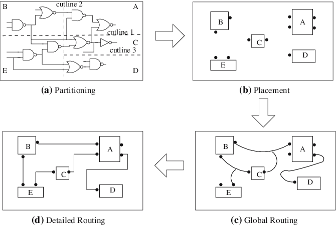
Modern SoC design has surpassed the scope manageable by a single engineer or a single CAD tool session. Attempting to handle it with a flat design approach leads to memory shortages, runtimes spanning weeks, and unresolvable timing issues.
Therefore, Partitioning is the first step in physical design and a strategic architectural phase that determines the success of the entire project.
Partitioning units are typically defined based on runtime. For example, criteria like "Let's ensure our Timing ECO has a runtime capable of running at least once per day."
1.1 Hierarchical Design
Partitioning applies the "Divide and Conquer" principle to system design. Design methodologies are broadly categorized into Top-Down and Bottom-Up approaches.
- Top-Down Partitioningol>
- The top-down approach divides the entire chip into large functional blocks at the system level. It then iteratively subdivides these into smaller modules, allocating PPSA to each subsystem starting from the Chip Top.
- It is commonly used at the System on Chip level.
- Bottom-Up Partitioning
- The bottom-up approach starts with small leaf cells or modules, builds them into subsystems, and finally assembles them at the top level.
- It is frequently used in reusable IP designs.
2. Advanced Partitioning Methodology
Recently, 'Pseudo-Flat' or 'Virtually Flat' approaches, which combine the advantages of Hierarchical and Flat methods, have gained attention.
Physically, it maintains a hierarchical structure through Partitioning, but during Timing Analysis or the CTS phase, the Tool perceives the entire design as Flat, eliminating inefficiencies at Block Boundaries.
2.2 Partitioning Algorithms & Optimization Metrics
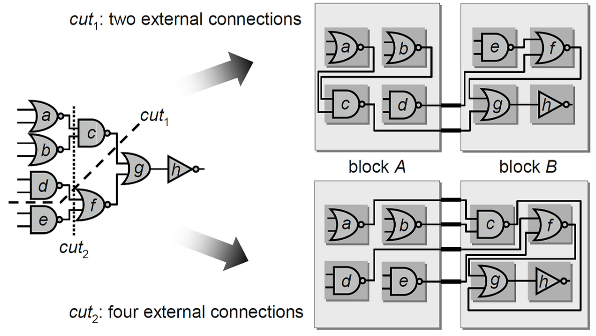
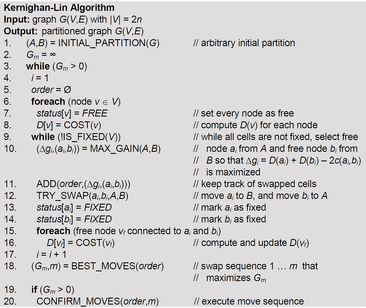
Partitioning must simultaneously consider Technical Constraints and Optimization Goals. The most representative algorithm is the Kernighan-Lin Algorithm. Here is the pseudo code.
- Min-Cut Principle: Interconnects must be minimized. Signals between blocks consume Routing Resources at the Top Level, and long Wire length causes Latency and Signal Integrity issues. Graph Partitioning Algorithms like Kernighan-Lin are used to minimize Cut size.
- Area Balance & Aspect Ratio: Each Partition must have a shape and size suitable for physical implementation. High Aspect Ratio or Rectilinear shapes reduce internal Placement & Routing efficiency. Typically, 1M to 3M instances is an appropriate size for a single block.
- Timing Budgeting: Partitioned blocks must have independent SDC. The Budgeting process, which determines how much of the Top-level path delay is allocated to internal logic, must be highly sophisticated. Excessive constraints lead to Area/Power overhead, while loose constraints cause Timing Violations during Top-level integration.
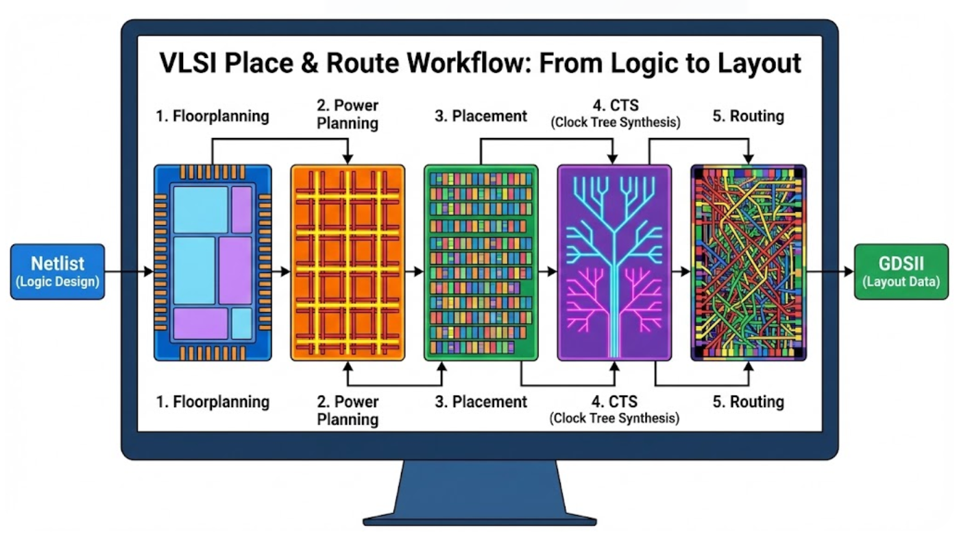
3. Floorplanning: The Structural Foundation
Floorplanning is the process of establishing the physical skeleton of the chip. Decisions made at this stage have an absolute impact on subsequent processes like Placement and Routing. An incorrect Floorplan can cause irreparable PPA Loss or Routing Congestion.
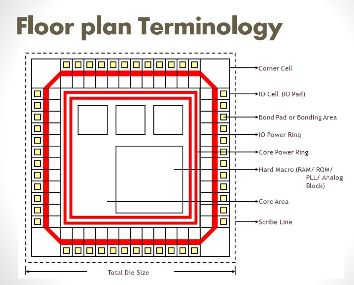
3.1 Core Area Definition & Geometry
- Aspect Ratio: This is the Width-to-Height ratio. Generally, the closer it is to 1.0 (square), the better the balance of Horizontal/Vertical Routing Resources, making it more efficient.
- However, due to the efficiency of Packaging, PCB Footprint, and Die Sawing efficiency may necessitate a rectangular shape, which can cause Congestion in specific directions. It is preferred to prioritize achieving a 1.0 ratio for high-frequency blocks like CPUs, GPUs, and NPUs first, followed by interface blocks.
- Utilization: The proportion of Standard Cells and Macros within the Core Area. Sizing, and Routing Margin. High densities exceeding 80% drastically increase Routing Congestion, making Timing ECO extremely difficult. It also causes DFM Yield degradation.
3.2 Macro Placement: Data Flow Visualization
Hard Macro (SRAM, PLL, ADC/DAC) placement requires the highest level of expertise. Macros are large and occupy specific Metal Layers, effectively acting as Routing Blockages.
Indeed, the three most critical factors in a Project, as stated by ASIC design engineers, are as follows:
- RTL Freeze (Complete RTL early to meet tape-out schedule)
- SDC Clean (Properly clean up unnecessary paths like false paths and MCPs, and apply appropriate constraints for each EDA flow to ensure stable signoff.)
- Golden Floor Planning (This determines the difficulty of chip utilization, hold time, SI, and DRC issues.)
[Macro Placement Strategies & Guidelines]
- Flyline Analysis: Analyze virtual connections between Macro-to-Macro and Macro-to-StdCell to optimize Data Flow. Ideally, place components so data flows straight from input to output.
- Peripheral Placement: Placing Macros at the Core Boundary or block periphery is standard practice to preserve the Center Area for Standard Cells and complex signal routing. Macros located centrally cause Detours, leading to severe Timing Delays.
- Macro Channel & Halo: Space is required between macros for Channel placement, where Power Strap or Clock Tree Buffer can be inserted. Additionally, a Keepout Margin (Halo) must be set to ensure Pin Accessibility and prevent localized Congestion.
Recently, AI-based floor planning methodologies are also being extensively researched.
2.3 I/O Planning and Pin Placement
Selecting the location of I/O pads or pins connecting the chip to the external world is also critical. When using wire-bonding packages, an I/O ring is formed around the chip perimeter. When using flip-chip packages, bumps are placed across the entire chip surface. The position of I/O pins acts as an anchor that determines the data flow direction of the internal logic, so it must be decided through close consultation with the PCB design team.EC%83%9D%EB%AA%85%EC%9D%84-%EB%B6%88%EC%96%B4%EB%84%A3%EB%8A%94-%ED%98%88%EA%B4%80-pdn-%EC%84%A4%EA%B3%84">3. Power Planning: The Lifeblood Vessels, PDN Design
Power Planning is the process of establishing the PDN (Power Delivery Network) to deliver stable and uniform power (VDD) and ground (VSS) throughout the chip. As we enter the era of fine-pitch processes, supply voltages are decreasing (threshold voltage reduction), while current density is rapidly increasing due to higher device density.content/images/2026/01/image-89.png" class="kg-image" alt="" loading="lazy" width="1077" height="730" srcset="https://www.vlsi.kr/content/images/size/w600/2026/01/image-89.png 600w, https://www.vlsi.kr/content/images/size/w1000/2026/01/image-89.png 1000w, https://www.vlsi.kr/content/images/2026/01/image-89.png 1077w" sizes="(min-width: 720px) 720px">
PowerPlanning, Ahmed Abdelazeem, Zagazig University
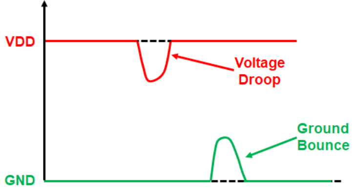
The resulting IR Drop and Electromigration (EM) issues have become the most significant risk factors causing chip reliability problems and Functional Failure.
3.1 Hierarchical Structure of PDN Architecture
An efficient power delivery network has a hierarchical mesh structure.
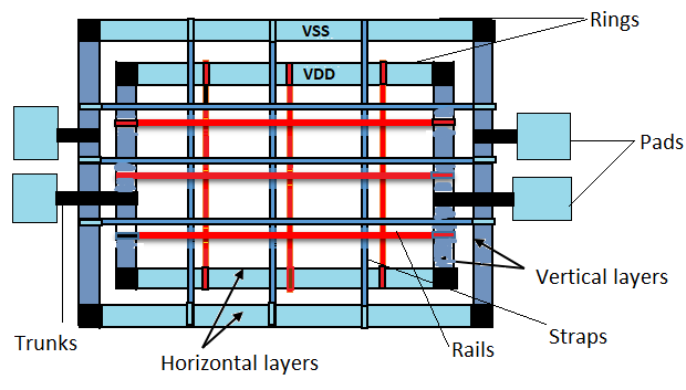
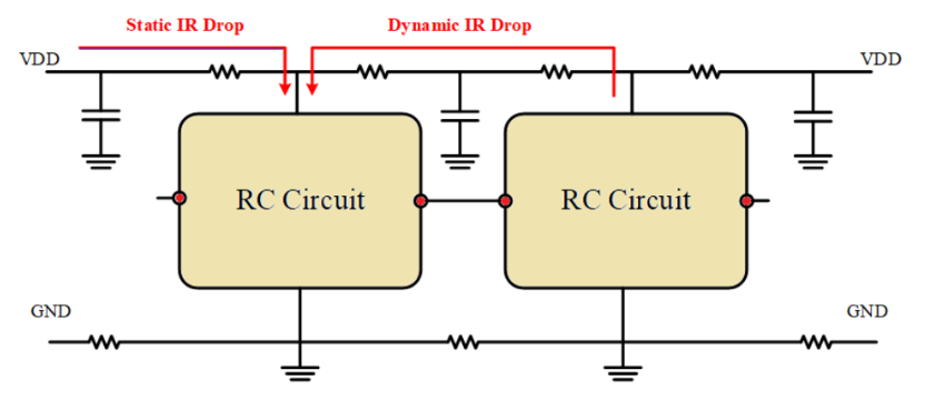
- Power Rings: Thick power lines that encircle the entire core perimeter of the chip or surround power-hungry macro blocks. They act as reservoirs where external power first arrives.
- Static IR Drop: This is the voltage drop when switching does not occur or when an average current flows.
- Solution - Reduce the total resistance of the power routing: This can be addressed by widening the stripe width or increasing the number of stripes to reduce parallel resistance, or by reducing the number of cells on this side.
- Dynamic IR Drop: This is a voltage drop caused by transient current occurring primarily during clock edges when numerous flip-flops and logic gates switch simultaneously. Combined with L(di/dt) noise, this causes severe voltage fluctuations, leading to timing delays or data malfunctions. Place a decap cell near the power pin to act as a local energy reservoir. When a sudden current demand occurs, it draws charge from the adjacent decap instead of a distant power pad, mitigating Dynamic IR Drop.
- Static IR Drop: This is the voltage drop when switching does not occur or when an average current flows.
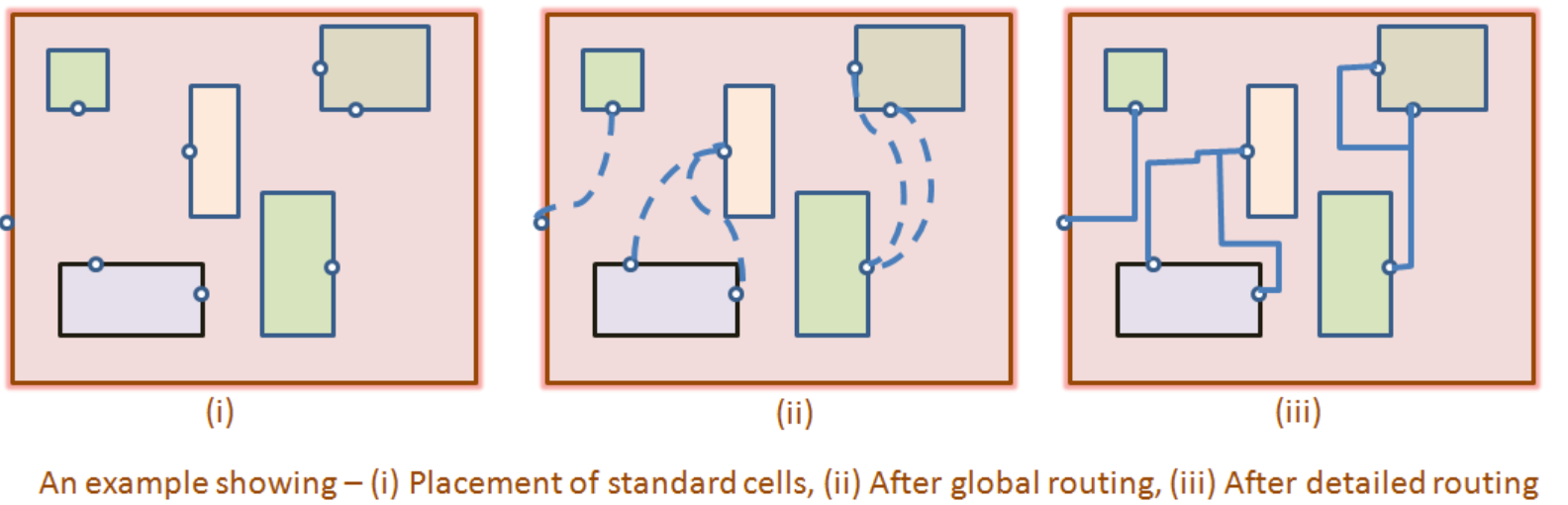
- Placement is the process of assigning the Logic Gates from the synthesized Netlist to specific coordinates (x, y) within the physical space defined by the Floorplan. The goal extends beyond simply placing cells; it aims to optimize Timing, Power, and Area while ensuring the subsequent Routing stage is feasible (Routable).
- Modern Placement Engines employ multi-stage optimization techniques to handle millions of cells.
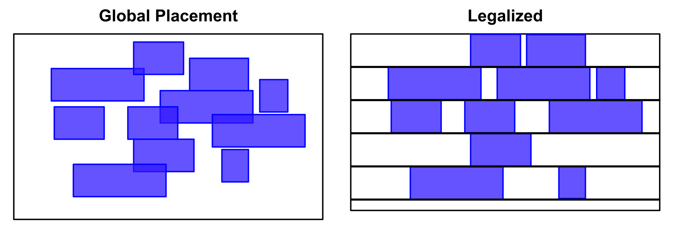
- Global Placement (Coarse Placement):
- Treats cells as mathematical Points rather than objects with size.
- Analytical Placement: Minimizes total Wirelength using Quadratic or Non-linear optimization techniques.
- Density Penalty / Electrostatic Force Model: Models cells as Charge that repel each other to prevent clustering, finding an equilibrium between minimizing Wirelength (attraction) and uniformizing Density (repulsion).
- As a result, cells are distributed in approximate positions, but Overlap exists and they are not aligned with the Standard Cell Row.
- Legalization:
- Based on the Global Placement results, all cells are moved to positions actually manufacturable.
- Cells are precisely aligned to the Standard Cell Row and Site Grid(Snap) and resolve Overlap. The key is to minimize Displacement to preserve the optimization results from the previous step.
- Detailed Placement: Performs fine-tuning after Legalization. Reduces Local Wirelength and improves Pin Accessibility by Swapping adjacent cells or moving empty spaces.li>
- Global Placement (Coarse Placement):
- Excessively high Pin Density in specific areas causes Congestion during the Routing phase, resulting in insufficient Track availability. which is the primary cause of DRC Violations (Short/Open).
- Cell Padding (Bloating): Virtual Padding is set around complex cells where Congestion is anticipated. This provides Porosity by securing physical distance, allowing routing to pass through.
- Congestion Map: Analyzes chip-wide congestion as a Heatmap using the Global Routing prediction model and applies the Cell Spreading technique to disperse cells in Hotspot areas.
- Clock Tree Synthesis (CTS) is the process of simultaneously and reliably delivering clock signals to the numerous Sequential Elements (Flip-flops) simultaneously and without corruption. The clock network accounts for 30-40% of the total Power Consumption, and its quality is a key factor determining the chip's Performance.
- The goal of CTS is to precisely control the following metrics.
- Latency: The absolute time from the clock source to the Flip-flop. Longer Latency significantly increases the impact of OCV (On-Chip Variation), leading to higher Timing Uncertainty, so it must be kept as short as possible. In other words, it is the Latency difference between Sink pins. Global Skew should ideally be 0 Skew, but the Useful Skew technique, which adjusts Local Skew between adjacent Registers to secure Setup/Hold Margin,strong> is increasingly utilized in recent times.
- Various topologies exist, ranging from traditional tree structures to mesh structures for high-performance computing.
- Routing is the step where pins of placed cells are physically connected with metal lines while adhering to design rules (DRC). This process is a continuation of the maze routing problem, which has NP-Hard complexity in mathematics.
- Routing proceeds step-by-step to control design complexity.
- Global Routing:
- Manages the entire chip by dividing it into GCell (Global Cell) regions.
- Before specifying concrete Track, it explores the GCell paths that must be traversed for Pin-to-Pin connections.
- The primary goal is Congestion management. It distributes congestion by comparing the Routing Capacity of each GCell Boundary with the actual Routing Demand and generating Detour paths.
- Track Assignment: Based on the Global Routing results, assigns each Net to a specific Track on a particular Metal Layer.
- Prioritizes straight routing to minimize Via usage and increase Routing Efficiency.
- Global Routing:
- Detailed Routing (Nano Routing):
- Creates the actual physical Shape within the assigned Track.
- Crosstalk Delay: When Aggressor and Victim traces Switching in opposite directions, the Coupling effect increases signal propagation time, causing Setup Violation. Conversely, Switching in the same direction accelerates transmission, causing Hold Violation.
- Crosstalk Noise (Glitch): This phenomenon occurs when an Aggressor's Switching induces an unwanted voltage spike (Glitch) while the Victim wiring is in a stationary state. This can invert the Logic Value, causing functional errors.
- Mitigation Techniques: Techniques such as ensuring Spacing, inserting Shielding lines between wiring, or adjusting the Drive Strength of the Aggressor Cell are employed.
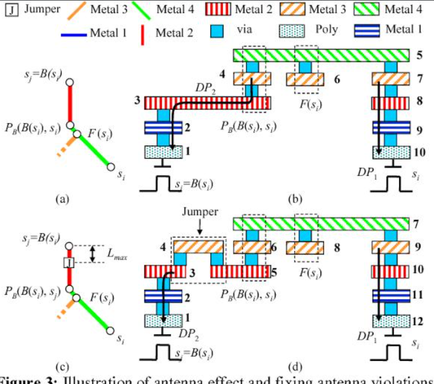
- Antenna Ratio: Managed by limiting the ratio of Area of wiring to Gate Area.
- Solutions:
- Jumper Insertion: Physically breaks the wiring length by inserting a Jumper that changes Layer in the middle of the wiring.
- Antenna Diode: Inserts a Reverse Diode near the Gate to safely discharge accumulated charge to the Substrate.
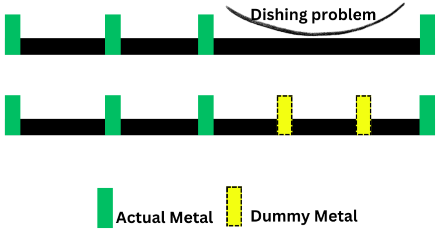
- Process:Fills empty spaces with 'Dummy Metal' pieces unrelated to circuit operation to achieve uniform metal density.
- Effect: Ensures chip flatness to prevent wiring defects and open circuits.
- Solutions:
- Diode Insertion: Insert a diode near the gate to drain accumulated charge to the Substrate.
- Metal Hopping (Jumping): Temporarily jump long traces to a higher metal layer, physically breaking the path where charge accumulates during the manufacturing sequence.
- Action: Where space permits, replace Single Vias (one via) with Double Vias (two vias) or more.
- DRC (Design Rule Check): Checks for violations of process rules
- LVS (Layout Versus Schematic): Verifies layout matches the schematic
- Creates the actual physical Shape within the assigned Track.
6.1 Routing Stages: From Path to Geometry
6. Routing: Finding the Path Through a Maze of Billions of Points
5.2 Clock Topology
5.1 Key Metrics of CTS
5. Clock Tree Synthesis (CTS): Temporal Synchronization
4.2 Congestion Management & Cell Padding
4.1 Placement Mechanism: Coarse to Fine
4. Placement
Creates fine Jog for Pin Access, generates Via, and checks and corrects compliance with thousands of DRC (Spacing, Width, Enclosure, etc.) rules.2 Signal Integrity (SI) & CrosstalkAs processes become finer, the ratio of Width to Thickness of traces increases. This exacerbates Crosstalk caused by Coupling Capacitance between adjacent traces.
6.3 Antenna Effect & Manufacturing Issues
During manufacturing, long metal wiring can act like an antenna and collect charge during the plasma etching step. If the accumulated charge discharges into the gate oxide of a connected transistor, the device can be permanently damaged.In the actual flow, Place_opt follows Place, and Route_opt follows Route, with opt continuously included in between steps.
7. Chip Finishing
Chip Finishing, the final step in the P&R (Place and Route) process, enhances the physical completeness of the designed chip to ensure it can be successfully Fabricated.While the previous step, Routing, completed the 'functional connections', Chip Finishing has a strong DFM (Design for Manufacturability) focus aimed at preventing process errors and increasing Yield.
7.1. Filler Cell Insertion (Space cell)
After Standard Cells are placed, empty spaces remain between cells.Leaving these spaces unfilled alters the substrate's potential characteristics. This is called a Density issue. These spaces are filled with 'Filler Cells' that have no logic function but serve a purely physical role, ensuring uniform characteristics.
7.2. Metal Fill (Dummy Metal)
During semiconductor fabrication, there is a CMP (Chemical Mechanical Polishing) process to grind the wafer surface flat. If the metal density across the entire chip is not uniform, some areas are ground more and others less, causing a phenomenon called dishing/erosion.
3. Antenna Effect Repair
During the Plasma Etching step in the process, long metal traces can accumulate charge like an antenna. If this accumulated charge discharges into the connected Gate Oxide, it can destroy the Gate.
4. Via Optimization (Redundant Via Insertion)
Vias, the holes connecting wiring layers, are the most vulnerable points with the highest probability of increased resistance or breakage (Open Defect) during the process.
5. Final Verification Preparation
Once this stage is complete, data is finally extracted (Stream Out) in GDSII (or OASIS) format,(Physical Verification).Chip Finishing does not alter the design's 'function', but it is the critical step that ensures the chip 'is born alive'.
Conclusion: P&R, the Ultimate Integration of Advanced Engineering
As examined, VLSI Physical Design is an organic and highly complex engineering process spanning from Partitioning to Chipfinish. The process of converting the logical design, the netlist, into the physical entity, GDSII, is not a simple transformation. It involves finding the optimal solution that satisfies all constraints: Physical Constraints (IR Drop, EM, Antenna), electrical constraints (Timing, SI, Crosstalk), and manufacturing process constraints (DRC, DFM).Particularly, the introduction of next-generation processes like FinFET and GAA presents P&R engineers with new dimensions of challenges, such as Quantized Cell Height, RDR, and Self-heating. Therefore, modern P&RR can never succeed by relying solely on the automation capabilities of EDA tools; it is essential for engineers to possess deep insight into the underlying algorithmic principles and physical phenomena at each stage.
Only the harmonious integration of Floorplan capabilities that read the data flow, PDN design capabilities that ensure power integrity, and ECO capabilities that meet timing requirements down to tens of picoseconds (ps) can guarantee the successful birth of a chip.
Power Stripes (Trunks): These are the main trunk lines that traverse the chip, delivering current deep into the core. They use the topmost thick metal layers to minimize resistance and are placed at appropriate pitchto control IR Drop. All standard cells are powered by connecting to these rails. A single via has high resistance and is vulnerable to electromagnetic interference (EMI), so connectivity must be enhanced using Via Arrays or Bar Vias.80%EC%9D%91-%EC%A0%84%EB%9E%B5">3.2 Physics of IR Drop and CountermeasuresIR Drop is the phenomenon where voltage drops (V=IR) when current (I) flows due to the resistance (R) of the power line itself.