
1. Introduction: Timing Integrity in Digital Integrated Circuit Design
In modern semiconductor design, particularly in the design flow of ASICs (Application Specific Integrated Circuits) integrating billions of transistors, RTL (Register Transfer Level) code must be implemented in actual silicon (GDSII). This requires not only functional correctness(Functional Correctness) must be guaranteed, along with physical constraints such as Timing, Power, and Noise.
Unlike Dynamic Simulation, which verifies circuit operation by applying an Input Vector, Static Timing Analysis is a technique that mathematically and statistically analyzes all paths in the circuit to verify that electrical signals are correctly transmitted within the specified clock frequency.
This overcomes the limitations of dynamic verification, where simulation time increases exponentially with circuit size, and is the only methodology capable of efficiently verifying all timing corners during the sign-off phase.
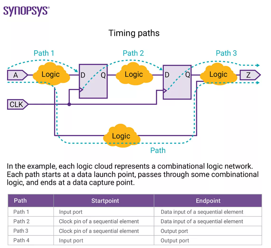
STA verifies Timing Paths.
The four elements of Timing Paths.
- -from Input port -to Data input of a sequential element
- -from Clock pin of a sequential element -to Data input of a sequential element
- -from Clock pin of a sequential element -to Output port
- -from Input port -to Output port
STA does not analyze the logical structure. It verifies all elements connected by the above four elements.
STA analyzes the timing values produced in each case by switching the input pin's signal from Low to High and High to Low.
Basic STA and library characterization use the Single Input Switching (SIS) technique. This method switches only one signal per STA.
Recently, Multi Input Switching (MIS) has also become a widely researched topic. This is because MIS is a real-world phenomenon, and when MIS occurs, the charging of the output load happens more quickly.
1.1 Why STA is 'Simpler' than Dynamic Simulation
Dynamic Simulation must calculate voltage changes for every transistor for every input Vector, but STA is a structural static approach that does not look at the logical structure.
- Vectorless: This is its greatest advantage. There's no need to consider circuit operation scenarios; only the worst and best timing for all paths need to be calculated.
- It works by switching all values on the input pins and storing the worst-case values.
- Graph-based Analysis: It converts the netlist into a Directed Acyclic Graph (DAG). You simply add the delays for each node (gate) and edge (net). Instead of solving complex SPICE differential equations, it transforms the problem into basic arithmetic operations based on the library.
- Coverage 100%: While simulation only verifies within the vector range we input, STA systematically scans all paths that exist structurally, all at once.
1.2 Why does STA produce results that are more 'Pessimistic' than reality?
There exists a "vector that won't actually flow in real silicon." Designers call this 'Pessimism'.
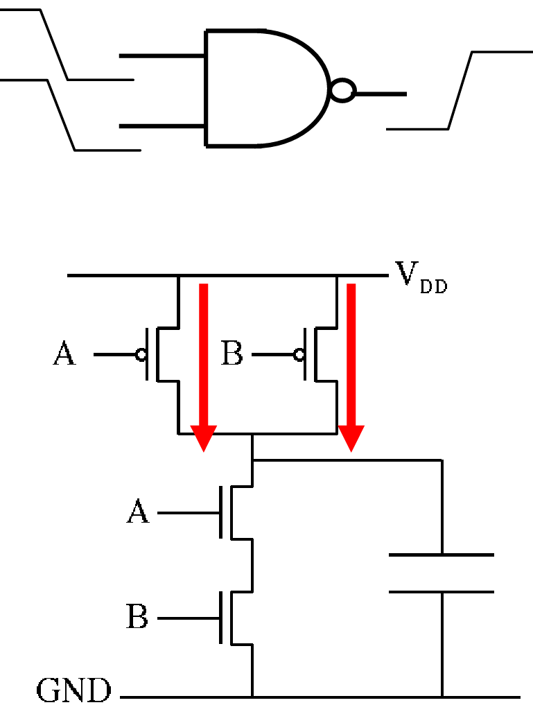
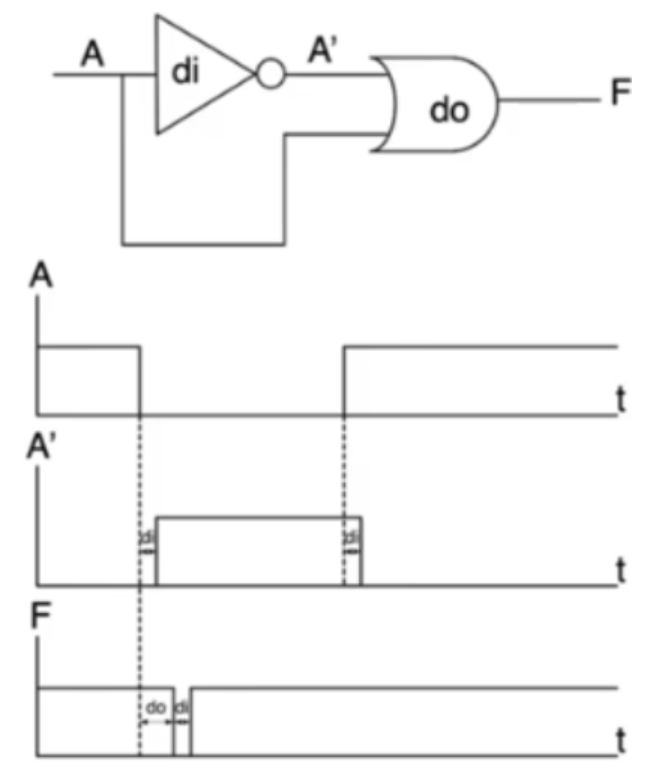
- False Path: STA calculates timing for paths where signals logically cannot flow, even though STA fails to recognize this. STA analyzes parts that won't actually occur or don't need verification.
For example, consider the Boolean calculation for D4/D in the figure below:
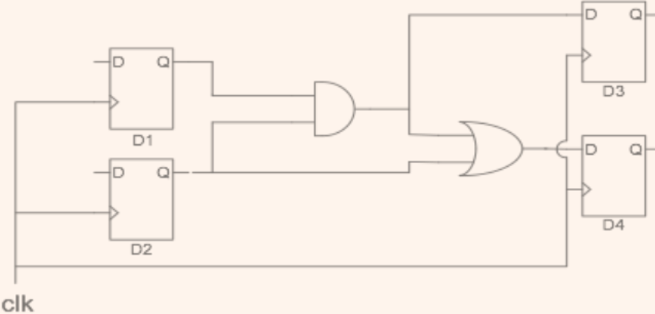
D4/D = (D1/Q & D2/Q) | (D2/Q)
This means that regardless of the value of D1/Q, the logic value of D4/D fluctuates based on the value of D2/Q.
- - The path from D1/D to D4/D is actually a timing path that requires no verification. However, STA recognizes even such timing paths as valid paths.
- Worst-case Corner Assumption: STA assumes the worst-case scenario for PVT corners. It considers extreme conditions like "all devices operate with slow launch paths and fast capture paths during setup time analysis."
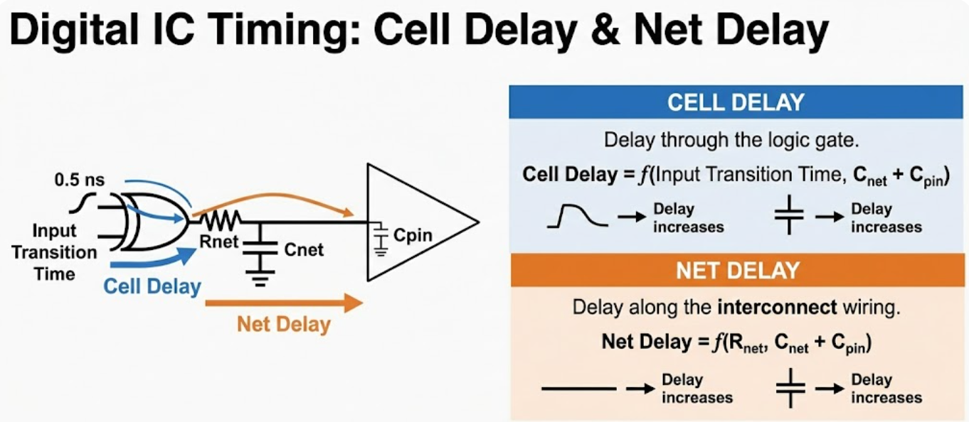
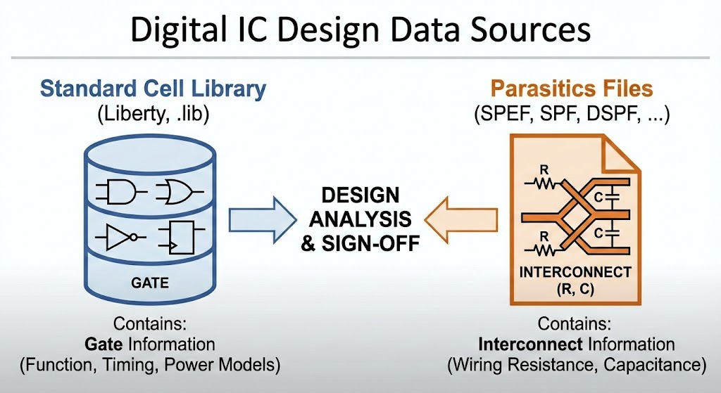
Gates are included in the Library (Liberty), and Interconnect information is contained in the Parasitics (SPEF, SPF, DSPF, ...) files.
2.1 Evolution of the Cell Delay Model: From NLDM to CCS/ECSMEC">2.1 Evolution of Cell Delay Models: From NLDM to CCS/ECSM
A cell library is a database that abstracts and stores gate characteristics. As processes have become finer, this modeling approach has advanced dramatically.
The most accurate representation is the actual silicon on a real-world wafer, followed by SPICE models that capture these characteristics. (SPICE involves differential-algebraic systems of equations, requiring immense computational resources.)
Therefore, for designs with a vast number of instances, only the material properties are characterized and stored in the library. During P&R, Synthesis, STA, etc., using only table traversal and interpolation.
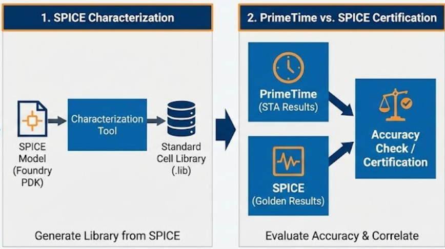
Characterizing SPICE as a library and then performing PrimeTime vs. SPICE accuracy evaluation (certification) are processes carried out by each process evaluation team.
NLDM, Non-Linear Delay Model
Primarily used in older processes above 90nm, the NLDM (Non-Linear Delay Model) takes the form of a Look-Up Table (LUT). It defines the cell delay and the output signal's Output Slew as a two-dimensional function of Input Slew and Output Load Capacitance.
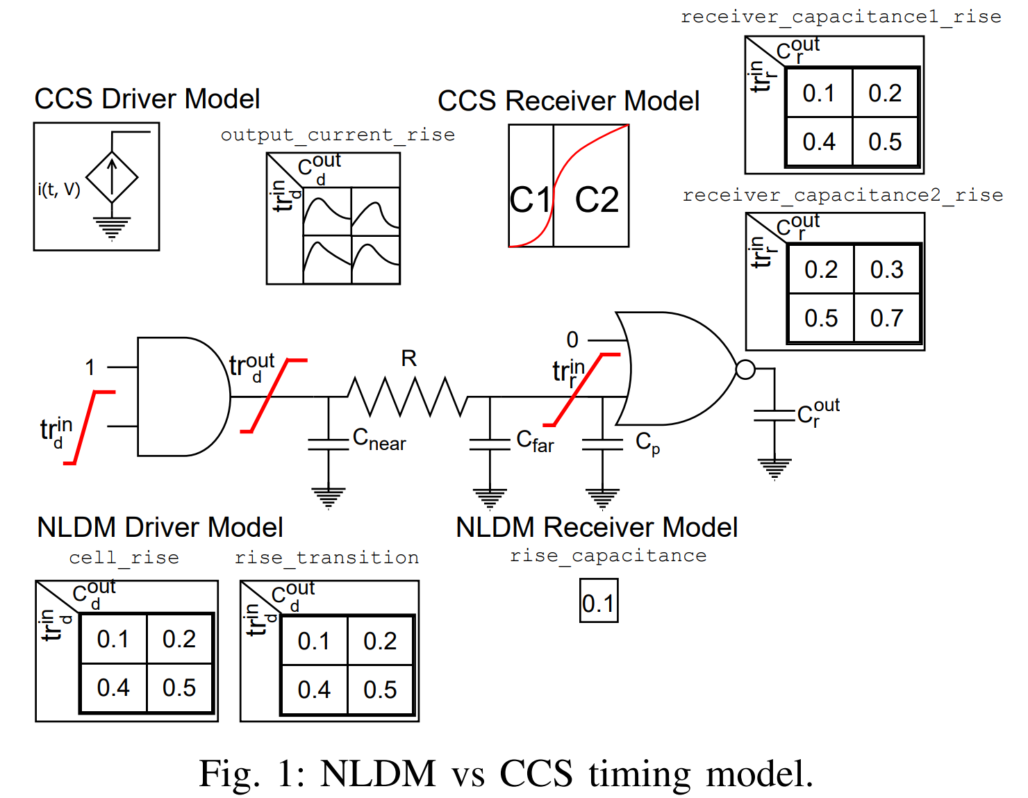
NLDM is a Voltage Source Thevenin Equivalent-based model that uses LUT lookup and interpolation methods instead of performing complex SPICE calculations directly. This offers the advantages of simplicity and speed.
However, as we entered sub-65nm fine processes, we discovered that adhering solely to this method resulted in a very poor error rate in PrimeTime - SPICE evaluation results.
Engineers observed that the output waveform developed a non-linear tail, deviating from a simple ramp shape, due to increased resistive interconnect components in the metal and a pronounced Miller effect in the transistors. This necessitated incorporating non-linear tail information into the existing NLDM.
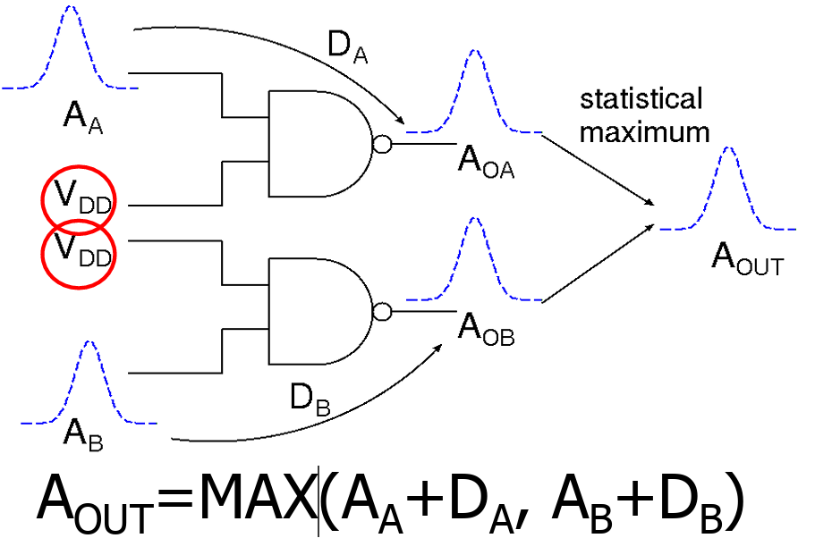
Current Source Models (CCS and ECSM)
Current-based models emerged to overcome these limitations.
- CCS (Composite Current Source): A model pioneered by Synopsys, it models the driver as a time-varying nonlinear current source. Specifically, to accurately reflect the Miller effect in the Receiver model, it finely models the input capacitance by splitting it into pre-switching (C1) and post-switching (C2) components. This dramatically improves accuracy in high-impedance nets (High-Z nets). (It is called the C1CN model.)
- ECSM (Effective Current Source Model): A model pioneered by Cadence, it models by back-calculating the effective current source based on the output voltage waveform.
The CCS model has spawned various models like CCS, CCST, CCSN, ... and various other models. Just as the CCS model emerged from NLDM, existing methods cannot simulate the characteristics of new processes, so various versions, like the BSIM model, continue to be researched.
2.2 Parasitic Extraction and Routing Delay
Once P&R is complete, metal routing is no longer an ideal conductor but a complex network of resistances and capacitances. The PEX (Parasitic Extraction) tool extracts R, L, and C values from the layout's geometric shapes and saves them as a SPEF (Standard Parasitic Exchange Format) file.
3. Mathematical Principles and Rules for Timing Verification: Setup and Hold
The core of STA is mathematically proving whether a data signal is captured within the correct time window relative to the clock signal. To achieve this, we examine two primary, opposing constraints: Setup time and Hold time. (There are also a few others, such as minimum pulse width, minimum period, and glitch noise.)
3.1 Setup Time Analysis: Max Delay Check
A Setup Violation occurs when data arrives later than the Active Edge of the next capture clock.
This is the primary factor determining the chip's Frequency. It assumes the Max Delay of the launch path (or data path).
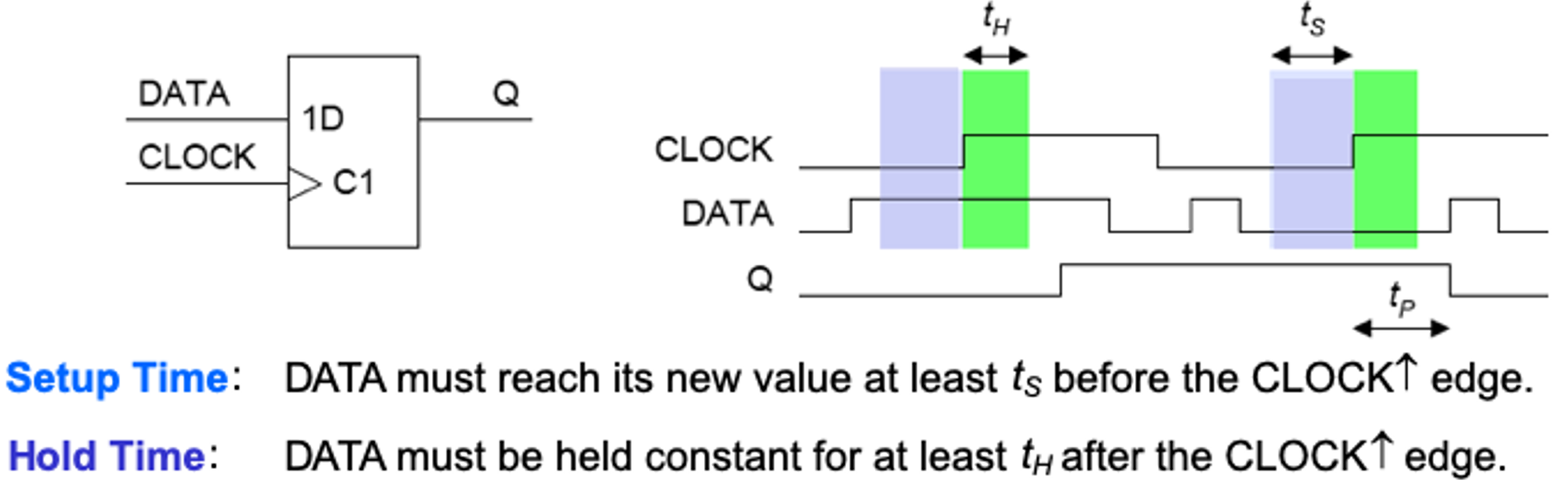
3.2 Hold Time Analysis: Min Delay Check
A Hold Violation occurs when data arrives earlier than the capture clock.
It occurs when data that should be captured at the current clock edge is overwritten by the next data (Race Condition) before capture, or when the data is not stably maintained for a certain period after capture. Hold analysis assumes the worst-case scenario (Min Delay).
4. Timing ECO (Engineering Change Order)
When Timing/Power/Noise violations occur, the common approach is to modify the cell to one with different physical characteristics (referred to as size_cell in the ECO process). If modifying the cell delay is not feasible, the interconnect layer is changed or the metal distance is adjusted. Swap to a cell with stronger drive strength (e.g., BUF_X1 to BUF_X4):
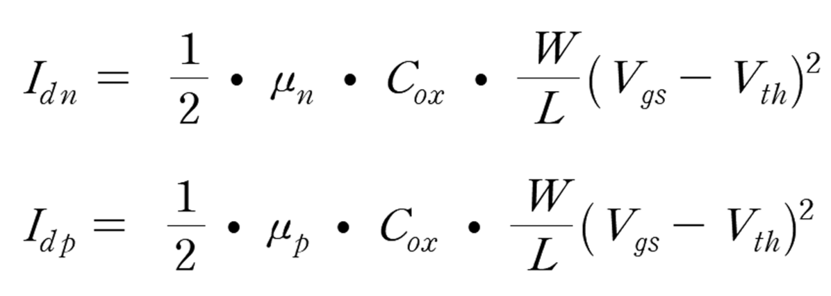
- Increase the transistor's W/L ratio to raise Idsat.
2) Swap to a cell with lower Vth:
- Lower the transistor's Vth value to increase Idsat.
3) Shorten the interconnect length:
- Reduce the area of metal capacitance to lower the C value.
4) Use a higher interconnect layer number:
- Use a layer with a larger distance between layers to reduce the C value.
Other methods include insert_buffer and ICG cloning.
4. Modeling Process Variation and Margin Elimination Strategies
As semiconductor processes become more refined, the phenomenon of non-uniform transistor performance due to wafer location, die-to-die variations, voltage drops, and temperature changes has intensified. Failure to account for this uncertainty leads to a sharp drop in yield.
4.1 PVT Corners Analysis
To ensure the chip can operate under all possible conditions, simulations are performed at corners combining extreme situations of Process, Voltage, and Temperature.
- Temperature Inversion Phenomenon: In past processes, higher temperatures reduced electron mobility, slowing cell performance.(-40°C). Therefore, during Setup analysis, both high-temperature and low-temperature corners must be verified.
- This explains why cross points appear when plotting tPD graphs versus voltage with HT and CT overlays.
4.2 From OCV to POCV: Reducing Excessive Pessimism
Single corner analysis alone is insufficient.EC%9D%B4%EA%B8%B0">4.2 From OCV to POCV: Reducing Excessive Pessimism
Single corner analysis alone cannot account for On-Chip Variation (OCV) within the die. Methodologies to address this have evolved towards reducing excessive design margins.
- OCV (On-Chip Variation): The most basic method applies a uniform Derating Factor across the entire chip. For example, it assumes worst-case scenarios by calculating the Launch Path as late (x1.05) and the Capture Path as early (x0.95). However, this pessimistic approach makes timing closure difficult as it conserves to physically impossible levels.(Pessimistic) approach to levels that are physically impossible, making timing closure difficult.
- AOCV (Advanced OCV): Considers Logic Depth and Distance. It utilizes the statistical property that deeper paths with more connected logic gates experience mutual cancellation (Averaging effect) of random variations, reducing the overall variation ratio. This allows for a smaller margin to be applied to deeper paths.
- POCV (Parametric OCV) / LVF (Liberty Variation Format): The standard for the latest 7nm and below processes. It models each cell's delay time not as a single value (Min/Max) but as a normal distribution with mean and standard deviation. The STA tool statistically calculates the cumulative delay distribution across the entire path (Statistical STA), dramatically reducing unnecessary margins.li>
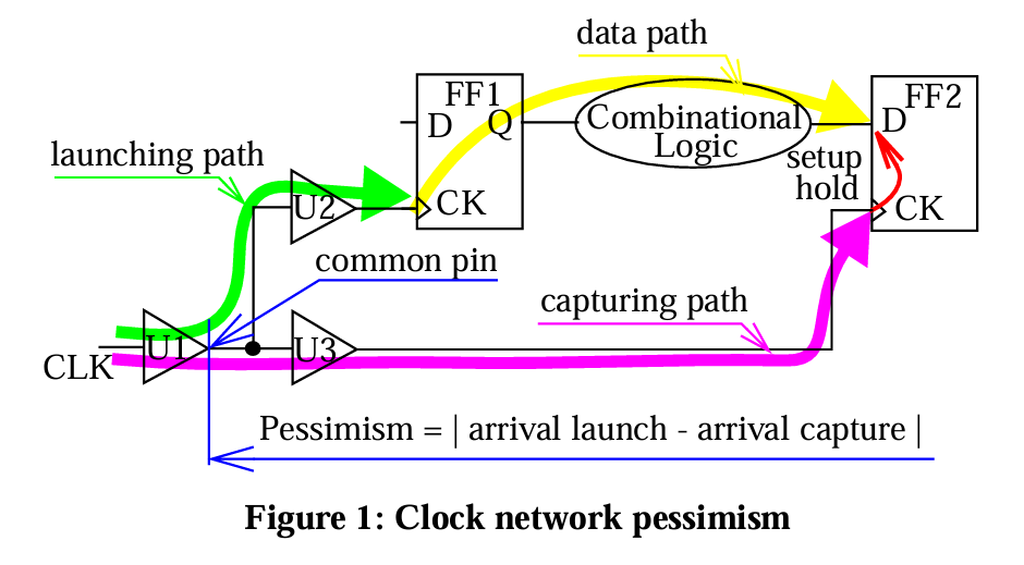
4.3 CRPR (Clock Reconvergence Pessimism Removal)
In a structure where the clock tree branches from a common source and reconverges on the data path(Reconvergent Path), a contradiction arises where buffers on the Common Path are physically a single cell but are calculated differently during OCV analysis as the Launch path (Late) and the Capture path (Early).
The process that removes this non-physical pessimism is CPPR (Common Path Pessimism Removal) or CRPR. CRPR is a crucial means of securing slack in timing closure.
5. Strategic Creation and Interpretation of Design Constraints (SDC)
STA tools only understand the circuit's interconnections; they are unaware of the designer's intent or the external environment. Therefore, timing requirements must be clearly specified through SDC (Synopsys Design Constraints). Incorrect SDC creation directly leads to chip failure(False Positive/Negative).
6. Signal Integrity, Crosstalk, Noise Bump
As process nodes shrink below 130nm, the spacing between traces narrows and the height of metal traces increases (High Aspect Ratio). This creates a phenomenon where traces are not physically connected but are electromagnetically connected. This phenomenon is called Crosstalk.
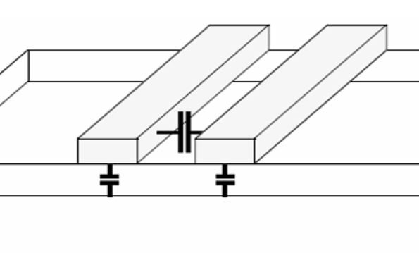
6.1 Crosstalk Delta Delay
When the Aggressor Net switches, the effect on the Victim Net's characteristics is called Crosstalk delta delay.
- Out-of-phase switching: When the aggressor rises and the victim falls, the signal transition speed slows down.
- In-phase switching: When both signals move in the same direction, the signal transition speed increases.
6.2 Noise Bump and Glitch Noise
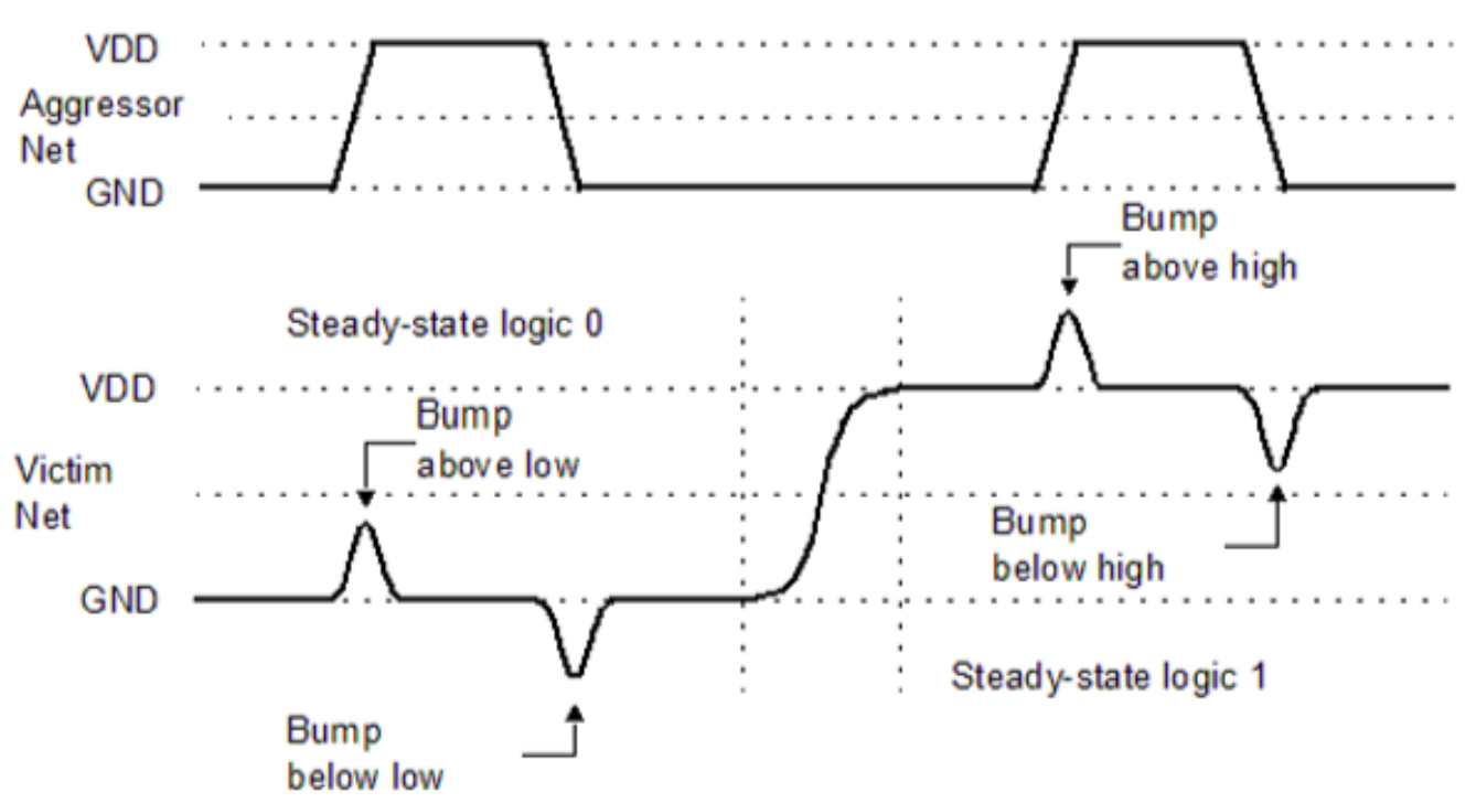
Crosstalk delta delay and its causes are similar.
- Crosstalk delta delay: Analyzing the timing impact of coupling capacitance and aggressor
- Noise bump & Glitch noise: Analyze whether coupling capacitance and aggressor affect function
Strong switching by the aggressor can induce unwanted voltage peak glitches on the stationary victim net.
Here, we analyze the above-low and Below High.
If the glitch's magnitude violates the input logic threshold rule of the next stage gate, a functional failure occurs where the logic value inverts.
- Glitch Propagation: A generated glitch can be attenuated or amplified as it passes through logic gates. STA tools analyze the glitch's Height and Width to determine whether it propagates to the input stage of the final flip-flop and affects the data.
It is important not to confuse Logic glitch (Static hazard Functional glitch) with Glitch Noise. Glitch noise is ultimately related to "Coupling capacitors and aggressors".
Logic glitches primarily occur due to timing imbalances in the signal path, leading to Race Conditions.
At the timing closure stage, we use PBA (Path Based Analysis). PBA follows the actual specific path and recalculates the exact slew. Typically, performing PBA on paths that violated in GBA often improves slack.
Even if a path violates in GBA, if it passes in PBA, that path is signoff-ready.
9. Conclusion
Through this research report, we confirmed that STA is not merely a 'check' process, but a sophisticated verification system combining semiconductor physics, statistics, and circuit theory.
- SPICE for simulating silicon characteristics,
- Libraries extracting only essential information from SPICE
- STA methodologies for utilizing these libraries.
The evolution from NLDM to current source models (CCS/ECSM), the introduction of statistical methodologies from OCV to POCV, and the importance of signal integrity analysis are all engineering solutions developed to overcome the uncertainties of fine-pitch processes.
The role of the signoff engineer is to create the signoff guide and ultimately determine whether tape-out is feasible or not.