

Chip design, particularly for modern, complex System on Chip (SoC) designs, is growing on an unimaginable scale.
In the past, it was possible to fit an entire design into a single Verilog netlist and process it with an EDA tool. Now, that approach leads to several problems.

Massive Designs, New Challenges
The explosive growth in design size puts an immense strain on EDA tools. Trying to process everything in a single netlist runs into the following issues:
- EDA Tool Processing Limits: Analyzing and optimizing designs with hundreds of millions, or even billions, of gates as a single unit pushes tool memory and CPU resources to their limits. You might hit the tool's specification limits or even the memory limits of your own computer.
- Unrealistic Runtime: Processing everything at once can take days or even weeks for tasks like timing analysis, and place and route. This can be fatal for a development schedule.
- Debugging and Management Difficulty: Finding and fixing a timing violation or a functional error in a giant, monolithic design is like finding a needle in a haystack. It also makes it difficult for multiple people to collaborate.
In engineering, we solve this kind of problem with "Divide and Conquer."
The Solution
This is why even a single chip design is usually divided into multiple blocks. The method for dividing them is quite complex, but we can talk about that another time.
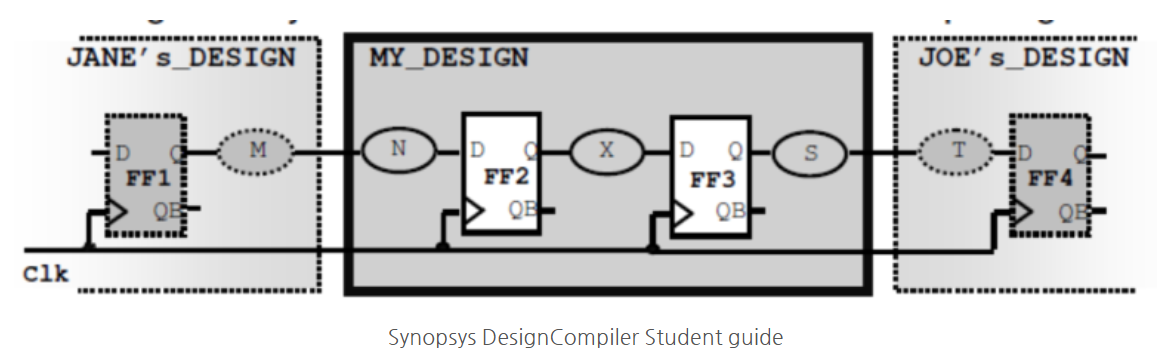
For example, let's say we have a design with four flip-flops, split into three blocks as shown below. Jane is responsible for the left block, Joe for the right block, and I handle the center design.
The content below is the core of this article, so even if it's difficult, please make sure to get it!
For the chip to function correctly at the top level,
all paths—FF1 -> FF2, FF2 -> FF3, and FF3 -> FF4—must meet setup and hold time requirements.
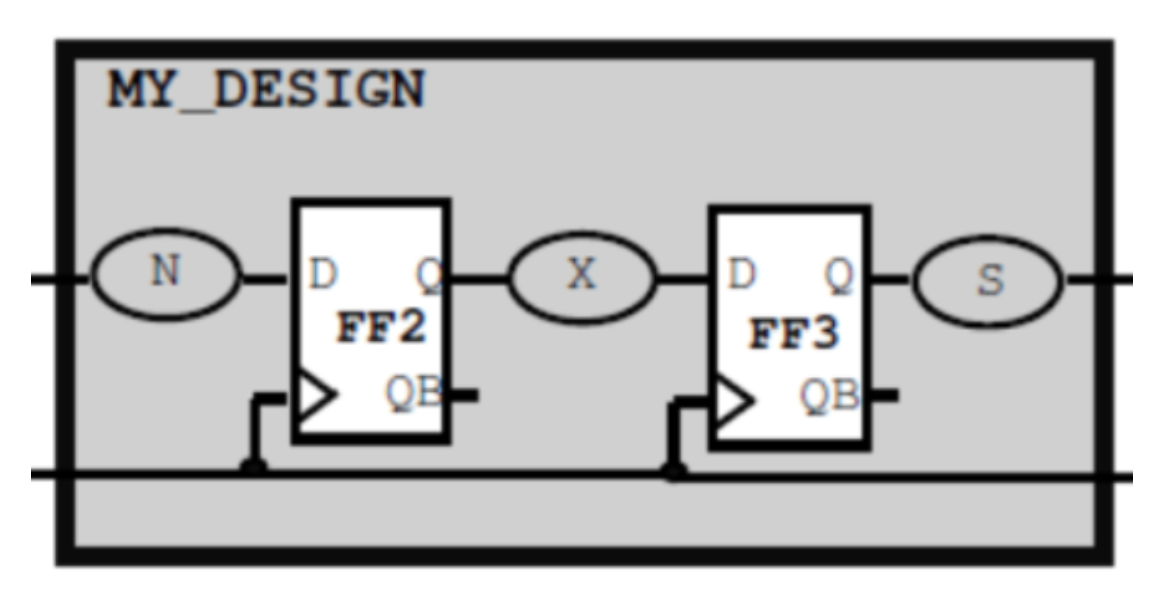
In my design, I can see the data path 'X' from FF2 to FF3, so I can perform timing verification for this path during physical design.
But how do you verify the paths from FF1 to FF2 and FF3 to FF4?
Input & Output Delay based on the clock frequency.
At the chip level, the setup time for the FF1 -> FF2 path is calculated roughly like this:
Setupslack=Clockperiod−datapath Setupslack=Clockperiod−[M+N]
However, in "My Design," I don't know the delay of M(Jane's DESIGN). So, I assume a delay for M and design my block accordingly.
M=Clockperiod×0.6
Setupslack=Clockperiod−[(Clock×0.6)+N] Setupslack=[Clockperiod×0.4]−N
This means I only need to design my block so that the value of N is less than or equal to Clockperiod × 0.4.
Similarly, Jane's design only needs to be made so that the value of M is less than or equal to Clockperiod × 0.4. At the chip level, the total setup slack would then be around Clockperiod×0.2.
Why 60%?
So, why exactly is 0.6 (or 60%) the specific value given for IO Delay?
Before top-level STA (Static Timing Analysis), using 60% is an unspoken rule of thumb. This is because there might be no margin for optimization in the I/O of the block you're interfacing with.
After running a top-level STA, you can adjust the IO Delay based on the available slack.