
The semiconductor industry represents the pinnacle of human technological civilization, yet it is also the most brutal test of capital. The physical effort required to integrate one more transistor is now tied to trillions of won in capital expenditures (CAPEX), and engineering success must cross the threshold of economic viability to be recognized as valuable.
Management Accounting is not merely a post-event bookkeeping exercise. It supports decisions on the 'semiconductor spec datasheet' where trillions of won in R&D funds are invested, and converts minute yield and PPA variations for setting PDK process parameters below 2nm into monetary value, proving management intuition with data—a highly strategic system.
1. Semiconductor Management and Financial Fundamentals
The essence of management accounting lies in generating valuable information for internal decision-makers.
Unlike financial accounting for external investors, it is forward-looking and focused on achieving the organization's strategic goals. The semiconductor industry's extreme volatility and fixed-cost-centric cost structure have driven the classical tools of management accounting to evolve into more sophisticated forms.
1.1. CVP
CVP (Cost-Volume-Profit) analysis is the most fundamental tool for evaluating the soundness of a semiconductor business model. For fabless companies, fixed costs carry the nature of sunk costs, making the securing of contribution margin to recover these costs a matter of survival.
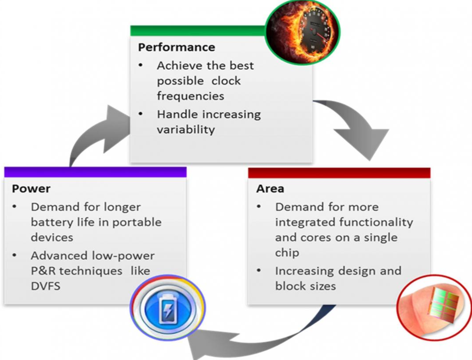
Profit = (Price - Variable Cost) * Quantity - Fixed Cost
For semiconductor engineers, this formula is not just numbers; it is synonymous with PPA (Power, Performance, Area) optimization
- Performance:Improved clock frequency enables product differentiation, leading to a premium in the market's ASP (Average Sales Price).
- Power: Power efficiency is a key variable that lowers the TCO (Total Cost of Ownership) for data center operators, thereby increasing customer retention rates.
- Area: Chip area determines the number of dies per wafer. Reducing die area lowers variable cost per unit, directly increasing contribution margin.
1.2. Activity-Based Costing (ABC) and Fab Operations
In modern semiconductor fabs with automation rates exceeding 95%, cost allocation based on direct labor costs loses its meaning. Activity-Based Costing (ABC) tracks costs based on specific resource-consuming activities, enabling precise measurement of product profitability.
Applying cost drivers to each activity pool example:
- Lithography: Number of exposures (EUV equipment usage time, mask cost allocation per layer)
- Etch & Decomposition: Process time and gas consumption (material consumption by FinFET, GAA structure)
- Metrology: Number of inspection points (In-line defect inspection and metrology time)
- EDS: Test time and probe wear (Die size and test items)
The ABC System acts as a filter for semiconductor companies when determining their product portfolio. It visualizes which products actually consume more equipment time, thereby filtering out 'false profitability'.
2. Financial Performance Management (FPM) and Value Creation Metrics: ROIC, EVA, WACC
In industries with extreme capital intensity, such as semiconductors, simple 'profit' can be misleading. The key is how much added value was created relative to the massive capital invested.
2.1. ROIC (Return On Invested Capital) and WACC (Weighted Average Cost of Capital)
The value of a semiconductor company is only created when its ROIC exceeds its cost of capital, WACC.
- NVIDIA's Model: Maintains a highly asset-efficient fabless model, achieving ROIC of approximately 25% or higher. This generates massive cash flow that can be reinvested into R&D.D.
- Intel's Crisis: During its transition into foundry business, CAPEX surged sharply, causing ROIC to drop to 7-10%. This directly led to a decline in market valuation.
But honestly, ROIC and ROE don't really resonate when you just look at them. Let's apply the DuPont framework.
If I recall correctly, ROE/ROIC alone are rather bland metrics, but the moment you break them down using DuPont, they become a "management decision-making tool".
Let me precisely recall the point that felt interesting during my MBA.
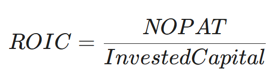
2.2 ROE / ROIC?
- ROE = Net Income / Equity
- ROIC = NOPAT / Invested Capital
At this stage: "So why did it increase?" "What did management do well?"
It's just a result metric, not a cause analysis
2.3 Core Idea of the DuPont Framework
Profit Margin × Asset Turnover × Equity Multiplier breaks down performance
This is the moment MBA students go "Oh!"
2.4 DuPont Decomposition of ROE (Classic)

Meaning Interpretation (Important)
- Profit Margin: Pricing power / Cost control effectiveness?
- Asset Turnover: Were assets utilized efficiently?
- Equity Multiplier: How much leverage was employed?
ROE increase = Can distinguish whether it's from "earning money well" or "increasing debt"
-ROIC-Dupont-Earnings">2.5 ROIC is also fundamentally a DuPont mindset
ROIC is typically broken down like this:

- ROIC is de-leveraged
- Pure business model competitiveness
ROIC is a more honest indicator of whether a company is truly performing well
- Company A: ROE ↑
→ Margin ↓, Turnover ↑: Low-margin high-volume sales strategy - Company B: ROE ↑
→ Margin ↑, Turnover ↓: Premium / Monopoly strategy - Company C: ROE ↑
→ Equity Multiplier ↑: Increased Financial Risk
A single number begins to reveal the business model, risk, and strategy
2.6. EVA (Economic Value Added) and Strategic Capital Allocation
EVA is the actual profit remaining after deducting all capital costs.
EVA = NOPAT - (Invested Capital * WACC)
For semiconductor division managers, EVA provides a powerful incentive to optimize Invested Capital by reducing unnecessary inventory and increasing equipment utilization rates.
For example, when considering the addition of hundreds of billions of won worth of test equipment, evaluating whether the resulting Incremental EVA is positive (+) helps prevent overinvestment.
3. Technology-Management Convergence Analysis: The Semiconductor Industry's Unique Characteristics and Management Accounting Responses
The semiconductor industry possesses four critical financial characteristics that distinguish it from other manufacturing sectors.
3.1. Capitalization vs. Expensing of R&D Costs and Delay Effects
Semiconductor companies typically invest 9% to 34% of their revenue in R&D.
- EDA / IP Companies: Classified as a high R&D industry, spending over 30% of revenue on R&D.&D.
- Foundry: On average, spends about 10% of revenue on R&D, with a structure where CapEx is significantly larger than R&D.
- Accounting Treatment: R&D is expensed as incurred, but its economic substance is an 'intangible asset' that secures future revenue.
- Lag Effect: A significant time lag exists between the timing of R&D investment and the actual realization of profits. Management accounting models this lag effect to track the effectiveness of investments.
- R&D Valuation: The market recognizes fabless companies' R&D expenditures not as costs but as value-creating assets, granting higher multiples to companies with high R&D intensity.
3.2. The Economics of Depreciation Expense Ratio and Utilization Rate
In the Foundry Business, over 70% of fixed costs are equipment depreciation expenses.
- Idle Capacity: Downtime at a fab represents hundreds of millions of won in lost opportunity per hour. Management accounting separately measures idle production capacity to manage cost increases resulting from reduced utilization rates.
- Beyond simple utilization rates, OEE integrates availability, performance, and quality, linking this metric to financial value.
-%ED%99%94%ED%8F%90-%EA%B0%80%EC%B9%98-%ED%99%98%EC%82%B0-loss-matrix">3.3. Converting Yield Volatility to Monetary Value: "Loss Matrix"
For engineers, yield is the outcome of process optimization, but for management, yield is 'Gross Margin' itself.
- Real-world example: When data shows yield losses at a specific process step amount to $X annually, finance and engineering can prioritize resource allocation using the same language.
① Verification (Bug is a Killer)
Unlike software, semiconductors cannot be 'patched'. If bugs are found after the chip is produced, money and time vanish into thin air. It's simply worthless.
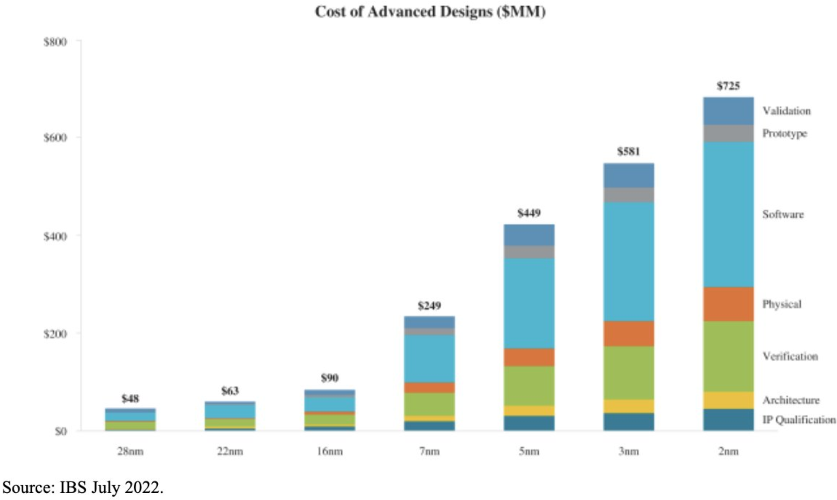
For reference, a single 2nm chip project incurs nearly $725M in design costs. This structure means even a mid-sized company can go bankrupt from a single silicon re-spin.
Even if we find a bug and fix it to quickly tape out again,
foundries typically only accept advance reservations for one year's worth of production. and only accept process reservations for the year after that. If a bug occurs requiring a silicon re-spin, even if you tape-out immediately, you should expect an additional 1.5 years until fab-out.
Since the semiconductor industry doubles its integration density every two years, a delay of 1.5 years means you'll be completely overtaken by competitors. If a major bug occurs... the project will likely become effectively abandoned.
If this bug is discovered after the product is sold to customers, it becomes an even bigger problem.
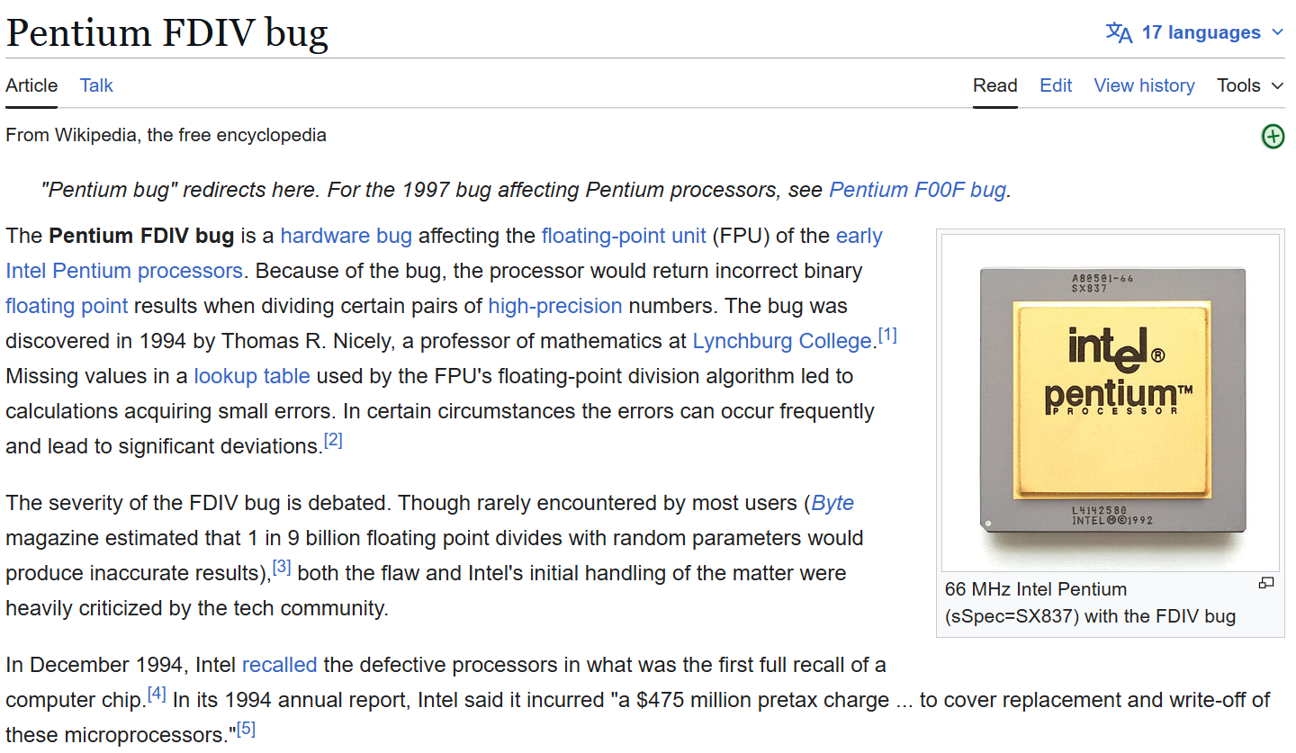
In 1994, the Intel Pentium chip debuted boasting of being a "math genius," but it had a critical bug in its floating-point division (FDIV) functionality.
Five entries in the chip's "lookup table" for fast division were mistakenly set to zero. This was due to a scripting error by the table creator, who entered "0" instead of "2". Consequently, in calculations like 4195835 ÷ 3145727, the Pentium outputted the absurd value of 256.
This happened in 1994. In an era like today, where semiconductor prices are skyrocketing and semiconductors are used in autonomous driving and artificial intelligence, what would happen if a bug caused someone to die? Even Big Tech might struggle to survive.
Ultimately, to win in the market, chips must be faster (Performance), consume less power (Power), and be smaller (Area).
If you're targeting CES 2030, PPA optimization is critical because you need to showcase the best AI performance and power efficiency of the era.
③ Time-to-Market (Release Timing - "CES won't wait for you")
No matter how good a chip is, it's meaningless if it comes out after the CES show ends.
The three most critical factors for an ASIC Project's TTM are:
- Design Freeze Timing (RTL Freeze): Finishing RTL design quickly allows for faster completion of Physical Design, which directly impacts PPA.
- SDC Clean: If you don't set things like false paths correctly, apply overly restrictive constraints, or place buffers in the wrong spots, you'll end up with bottlenecks in completely unnecessary places and fail to capture the actual critical paths.
- Golden Floorplan: A flawed floorplan leads to routing congestion hell, timing violations, shorts, PV issues, and ultimately spec downgrades.
4. Opportunity Cost and ROI of Time-to-Market
The semiconductor market largely operates based on conferences visible to end customers.
Therefore, it clearly shows where investment should be allocated at each stage.
For example, CES (Consumer Electronics Show) is a global consumer electronics show where the world focuses. Consumer electronics companies must showcase prototypes at this time. (Apple has its Apple Developer Conference, Google has Google I/O, and each company holds annual events.)
For example, let's assume we are preparing for CES 2030.
Phase 1: Spec-in & Architecture (~December 2026)
- Core: Secure PDKs (Process Design Kits) from each foundry, finalize the IP list, and complete evaluations.
- Additional Tasks: Sign NDAs with Foundry/EDA/IP companies and finalize the SoC architecture.
Phase 2: 1st RTL-to-GDS (Jan 2027 ~ Dec 2027)
- Key: Complete RTL design, Verification, Physical design, and Signoff must all be completed.
- The three most critical elements for successfully concluding an ASIC Project are as follows:
- Early Design Freeze (RTL Freeze)
- SDC Clean
- Golden Floorplan
- Additional Tasks: During this period, launch the Virtual Prototype and Emulation to enable the SW team to pre-develop the Compiler and Driver.
Phase 4: Bring-up & 2nd Tape-out (August 2028 ~ February 2029)
- Actual Process: Once chips are produced, we receive sample wafers during testing to verify 'Alive' status for 1-2 months, diagnose yield issues, and measure PPA.li>
- Revision: Minor bugs discovered here are fixed, and the final production-ready (B0) Tape-out to push PPA and Yield to their limits must be conducted in January-February 2029.
Step 5: Final Chip Acquisition and Productization (August 2029 ~ December 2029)
- Final Chip Arrival: Final chip (B0) acquisition around August 2029.
- System Integration:The next four months will be hellish debugging. At this stage, there's no going back even if bugs surface. We must complete debugging, boot the system, mount the chip on the board, integrate it into the mechanical assembly, run the CES exhibition scenario (demo).
Management accounting calculates the 'opportunity cost due to launch delays' to demonstrate the financial justification for the engineering team's actions to reduce risk, such as purchasing expensive external EDA tools, IP, or adding personnel.
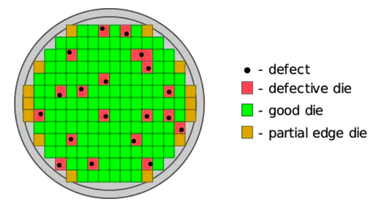
From a management accounting perspective, this isn't "defect handling." It's a joint product problem where multiple grades of product simultaneously emerge from a common input. In other words, the wafer cost has already been incurred (mostly sunk), and subsequent decisions shift to "which bin to sell as which SKU to maximize contribution margin."
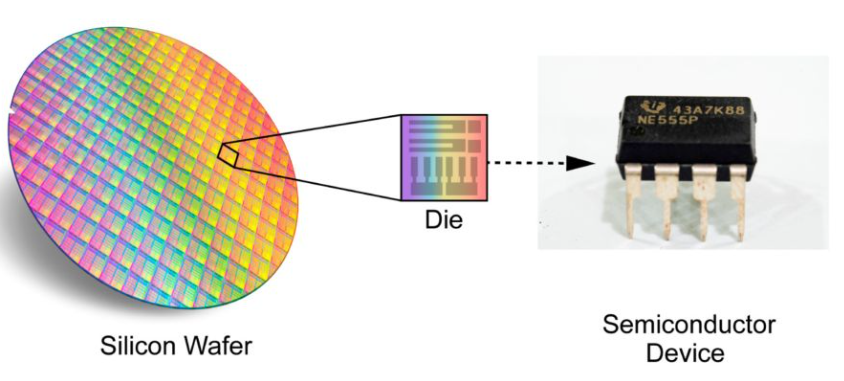
1) The Essence of Cost: The unit price of a 'good die' is determined by yield
Simply summarized,
- Cost per good die ≈ Wafer cost / (Dies per wafer × Yield)
Here, even a 1–2% fluctuation in yield causes the unit price to fluctuate significantly. Treating this volatility as mere "scrap" destroys gross margin. Therefore, companies convert the yield distribution itself into a sales distribution: the top bin becomes premium SKUs, the bottom bin becomes entry-level SKUs.
2) Pricing and Portfolio Strategy: Turning "Quality Variance" into a "Price Ladder"
From an MBA perspective, a binning-based portfolio simultaneously achieves the following:
- Capacity utilization: Allows selling lower-grade dies, increasing revenue recovery relative to wafer input (capacity).
- Price discrimination: Bins with ample performance and power headroom justify premium pricing.
- Portfolio fence: Protects the value of higher-tier SKUs while expanding the market with lower-tier SKUs.
- Variance absorption: Absorbs yield variance through sales mix ("converts the risk of cost spikes" into "SKU mix changes").
3) Management Accounting Details: Wafer Cost Allocation Simplifies Using NRV
Strictly speaking, wafer costs (common costs) must be allocated to each bin/SKU. The commonly used accounting approach for this is the NRV (Net Realizable Value) method:
- Joint costs are allocated based on the value obtained by subtracting additional separable costs from each product's final selling value.
- When directly applied to semiconductors, this creates a framework for viewing internal profit/loss as "bin-specific expected ASP – packaging/test/logistics differences".
and use DVFS/guard-banding to create dense speed/power bins.
In other words, mature operations incorporate" as an economic constraint is a mature operation.
5) Case hint: Same silicon, different SKUs
Apple's M1-based MacBook Air coexists with 7-core GPU / 8-core GPU variants in its specifications. This demonstrates that "SKUs with some cores disabled from the same die family" officially exist.
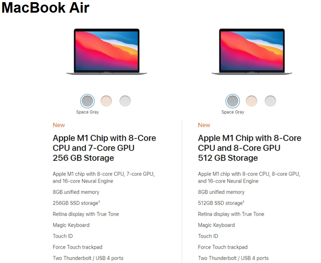
- Apple M1 (MacBook Air 2020)
- Within the same M1 family, 7-core GPU / 8-core GPU options coexist. (Apple Support)
- Apple A15 (iPhone 13 vs iPhone 13 Pro)
- iPhone 13: A15 + 4-core GPU (Apple Support)
- iPhone 13 Pro: A15 + 5-core GPU (Apple Support)
- That is, SKU tiering is separated by GPU core count within the same A15 line.
- Apple M2 (MacBook Air 2022)
- Base 8-core GPU configuration
- Optional 10-core GPU. (Apple Support)
- Apple M3 Pro (MacBook Pro 14-inch, 2023)
- 14-core GPU in the M3 Pro line
- 18-core GPU
- CPU also has 11/12-core options coexisting. (Apple Support)
- M3 Pro line features 14-core GPU
- Yield gains: Smaller dies have a lower defect probability, increasing overall system yield.
- Exponential increase in packaging costs: Conversely, packaging costs can account for 30% to 46% of total costs. Management accounting must calculate this trade-off point to propose the optimal chiplet partitioning strategy.
Apple M3 Pro (MacBook Pro 14-inch, 2023)Binning is not a "trick to sell defective products," but a mechanism that converts process variability (yield distribution) into product portfolio and pricing (revenue distribution).
6. Future Outlook: Strategic Responses to the Chiplet Era and Surge in CAPEX
As semiconductor miniaturization advances below 2nm and the adoption of High-NA EUV beyond EUV becomes visible, the role of management accounting becomes increasingly critical.
6.1. Cost Functions of Chiplets and Heterogeneous Integration
Chiplet technology, which breaks down massive monolithic designs into smaller chiplets for packaging, fundamentally alters the manufacturing cost structure.Semiconductor integration density has evolved following Moore's Law (doubling every two years). but over time, while integration doubled every two years, yield deteriorated and process costs increased significantly.
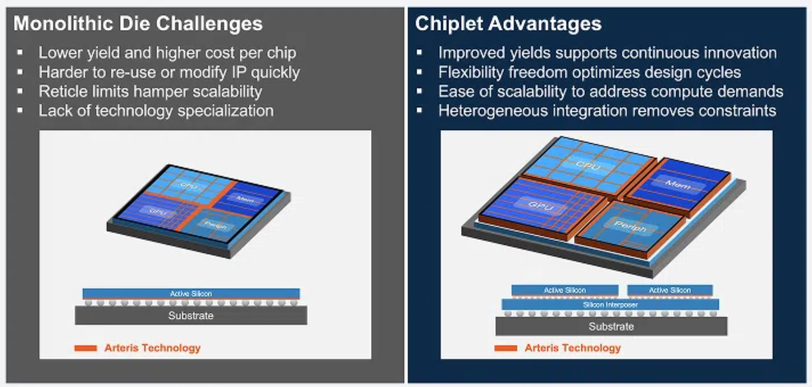
Ultimately, methods like 3D-IC or Chiplet are being adopted by splitting into smaller dies.
6.2. Precision Control of CAPEX and Management of CHIPS Act Subsidies
As the construction cost of a single fab exceeds $10-20 billion, the financial impact of government subsidies (such as the CHIPS Act) and the effect of subsidy conditions (like profit sharing) on WACC and capital budgeting must be precisely modeled in advance.
7. Conclusion: The Perfect Union of Silicon and Numbers
In the semiconductor industry, engineering defines 'what is possible,' while management accounting determines 'what must be done.' As we advance into the era of ultra-fine processes, economic constraints are increasingly likely to determine a company's fate over technical challenges.The reason semiconductor executives must possess semiconductor knowledge and the compass of management accounting is clearBecause every gate we design, every process step we optimize, ultimately connects to trillions of won in capital expenditures and becomes a variable determining the company's ROIC and shareholder value. 'Silicon economics' is no longer an option; it is an essential capability for survival.