![[VLSI CAD] Why Optimization is Hard: NP-hard, heuristic, AI EDA](https://images.unsplash.com/photo-1581089778245-3ce67677f718?crop=entropy&cs=tinysrgb&fit=max&fm=jpg&ixid=M3wxMTc3M3wwfDF8c2VhcmNofDE3fHxtYXRofGVufDB8fHx8MTc2NzI0MzQ1MXww&ixlib=rb-4.1.0&q=80&w=1200)
TL;DR
- Many of the core optimization problems in semiconductor design are NP-hard / NP-Complete / PSPACE-complete, so algorithms that guarantee an "optimal solution" are virtually unprofitable at scale (e.g., even if there are only 40 cases of 2, there are 1 trillion cases)
- This is why EDA tools are designed from the ground up to be heuristic + approximation + iterative improvement. This is not because "the tools suck," but because of the problem nature.
- AI/ML does not efficiently find "optimal" solutions to NP-hard problems. Instead, they actually benefit by guiding, automating, and narrowing the problem with models.
1) Physical Design: Why is it NP-hard
The most classic "hard" problem in Logic Synthesis, the first step of Physical Design, is two-level Boolean minimization. For example, the problem of finding the minimal SOP(DNF) that satisfies a truth table.
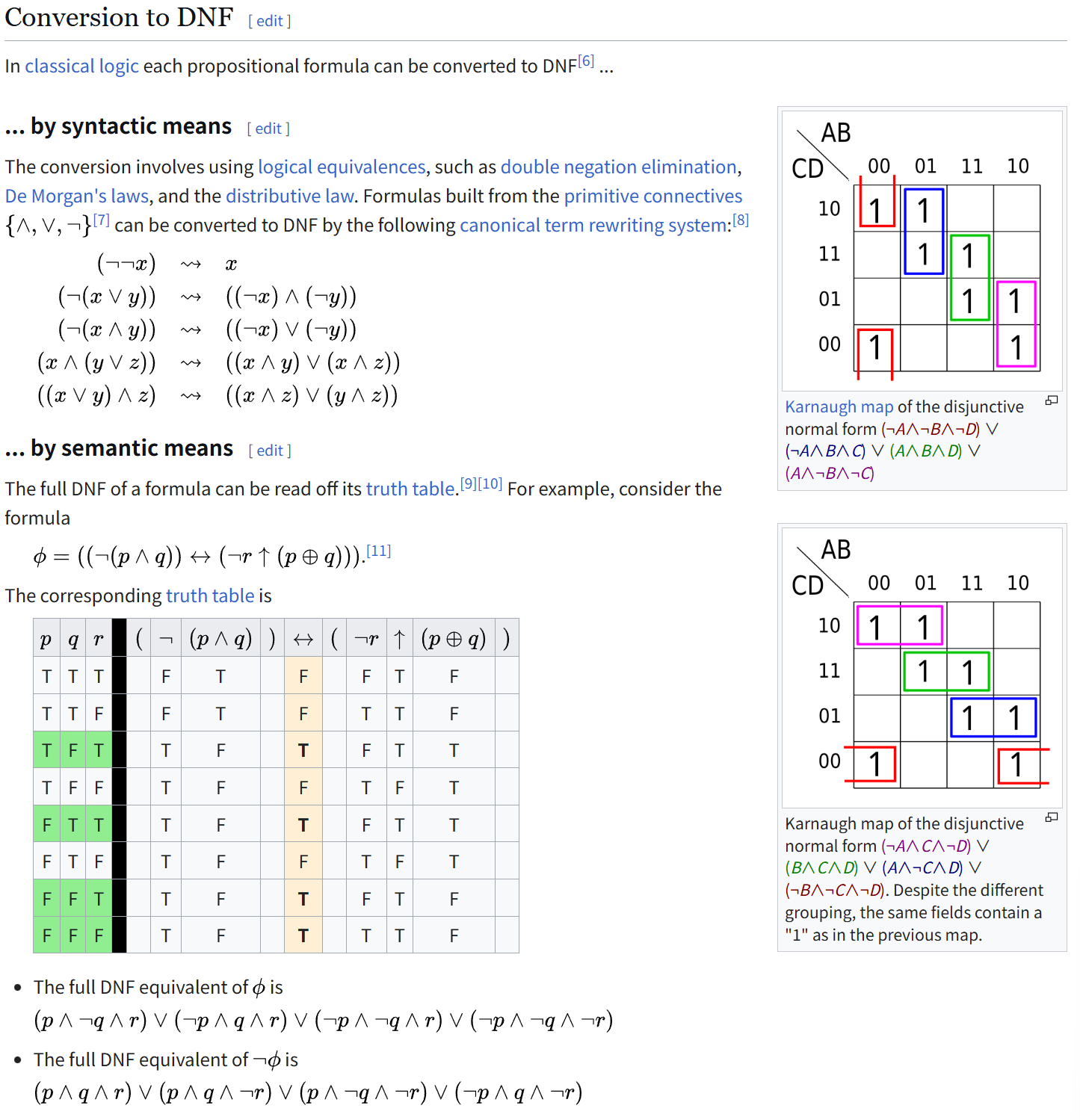
- The two-level Boolean minimization problem is known to be NP-complete.
Quine-McCluskey (QM) Case:
QM is a Boolean function simplification method taught in digital engineering.
- Goal: Cover a Boolean function with a minimal prime implicant,
- Procedure:
- Generate all prime implicants
- List all minterms
- Create Covering table (rows=minterm, columns=prime)
- Select minimum columns → minimum covering problem
👉 Problem 4.
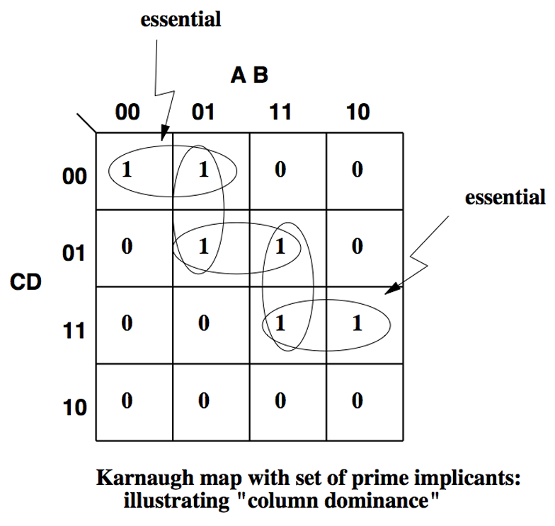
- In real circuits, the "set of possible candidate term combinations" is enormous, and QM has exponential complexity.
- The process of finding prime implicant combinations in QM's covering table falls into the set cover / exact cover structure, which is classically NP-complete.
The key point is this.
The reason why VLSI CAD (EDA Tool) is slow and difficult is not because the implementation is bad, but because the problem itself has a huge number of possible cases
That's why you hear "Can't you solve it with SATisfaction/Integer Linear Programming?", and it goes like this.
- SAT is NP-complete, ILP is also in the NP-hard category.
- That is, even if you change the format, it is still NP-complete and NP-hard.
2) Are there so many NP-Hard and NP-Complete in EDA steps?
The EDA flow is similar in nature even if the phases change.
"Place/select/connect components to optimize cost"
This structure is mostly NP-hard.
Below is a condensed version of "optimization goal → why hard".
2.1 Multi-level logic (AIG, DAG rewriting)
- Goal: Reduce gate count, depth, power proxy, etc.
- Why hard?: "global restructuring", which changes the circuit structure itself, becomes combinatorial search. Multi-output/minimization classes are also known to be NP-hard.
- Alternative solution: Local transform (algebraic rewriting, AIG rewriting)
2.2 Technology Mapping
- Goal: Minimize area/delay while mapping DAGs to standard cells or LUTs
- Why hard: Optimal mapping is known to be NP-hard for general DAGs
- Exception: Sometimes solved by DP if it is a tree structure, but it breaks because it is actually a DAG.
https://hjemmesider.diku.dk/~jegeblad/thesis.pdf
2.3 Placement
- Goal: minimize wirelength/congestion by placing cells in coordinates
- Simplification reduces to partitioning/bin packing and is known to be NP-hard.
- So reality: analytic placement + partitioning + heuristic refinement.
In addition, Routing, CTS, ... many things are NP problems.
3) decision vs optimization vs multi-objective
The reason why EDA is difficult is that what circuit designers want is not decision, but optimization, and it is also multi-objective.
- Decision problem: "Is it possible/impossible?" (e.g., is timing 1ns satisfactory?)
- Optimization problem: "What is the minimum/maximum?" (e.g., minimum wirelength deployment)
- Multi-objective: There are multiple objectives, such as Performance Power Area.
This is what it looks like in practice.
- "Timing must be met at all costs" (hard constraint)
- "Area/power must be reduced at a penalty" (soft constraint)
- And then you iterate and adjust the trade-offs.
In other words, EDA is not a game of "one right answer" from the beginning, but more of a game of designing constraints and compromises.
4) So heuristics are not 'optional', they are 'mandatory'
There are four reasons why heuristics are mandatory in EDA.
- Global optimal does not exist → accumulate local improvement:
- Global optimal is an optimal solution that lists all the cases and proves that there is no better case.
- Different levels of abstraction → What's good in logic synthesis may be bad in Placement.
- Cost function is messy → Nonlinear/nonconvex/stepped, so "canonical optimization" doesn't work well.
- incremental loop is the default → "modify→analyze→modify" is the essence, not "do it all at once."
Summary:
EDA tools are inherently "heuristic systems".
5) Where does AI/ML driven EDA really work?
It's dangerous to say that AI "solves" NP-hard problems, but IT communicators tend to over-hype it for the sake of views.
If you categorize it like this, it makes more sense. Although this one feels a bit lacking.
A) AI가 잘하는 영역: "predicting/scoring", not "solving"
- surrogate model: a predictor that replaces expensive simulation/analysis
- quickly predicts congestion, timing hotspots in placement/routing to guide navigation.
AI is stable when it enters the scoring function, not the solver.
B) AI가 실제로 돈 되는 영역: "AI does the work of multiple iterations of an EDA tool, minimizing designer effort."
This is one of the AI-EDA-like approaches of many EDA companies.
- Rather than changing the EDA engine itself, AI explores "options/flow/parameters" to reduce human tuning labor.
- This has a realistic ROI.
- The key here is search automation, not "AI reinventing placement".
C) Areas where the AI is currently weak: "Where we need 0% error"
- Signoff or formal verification requires a human level of proof to put the final stamp of approval. ML can help, but not replace."
- Solving an end-to-end SAT or designing an entire chip end-to-end is not generalizable/verifiable.
6) One-line assessment of popular AI-driven EDA examples
The following technologies are promising. However, there is a tendency to overestimate them in the media:
- Google RL macro placement (Nature): Impact was large. Reproducibility/comparisons are weak.
- DSO.ai / Cerebrus: A case of creating value by automating flow tuning rather than packaging AI as a "solver".
- agentic EDA / LLM: still "promising," but validation/accountability/data issues remain
7) Summary
- "AI solves NP-hard?"
- No. AI is not a way to find the optimal solution.
- "SAT+AI = optimal synthesis?"
- No. The search space remains the same.
- "cloud compute = solve? More computer resources?"
- No. Complexity is an exponential, so if the exponent is very large, you can't bring all the computers on the planet, and modern semiconductor designs have very large exponents.
- "AI driven EDA replaces designers?"
- Not yet. Requirements design + final verification + human accountability