
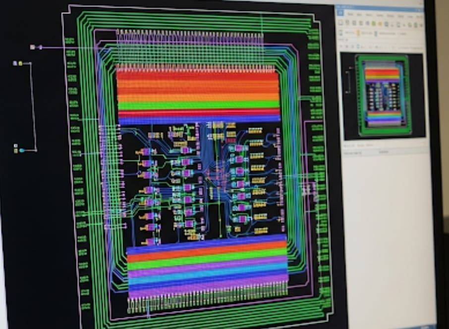
Do you have a semiconductor design engineer in your family? Before planning your Vacance? ask them for their 'Tape out' schedule.
The term “tape-out” harks back to the 1970s when engineers recorded design data on magnetic tapes and physically shipped them to foundries (Tapeout Origin). These tapes held the GDS files used to create photomasks for lithography.
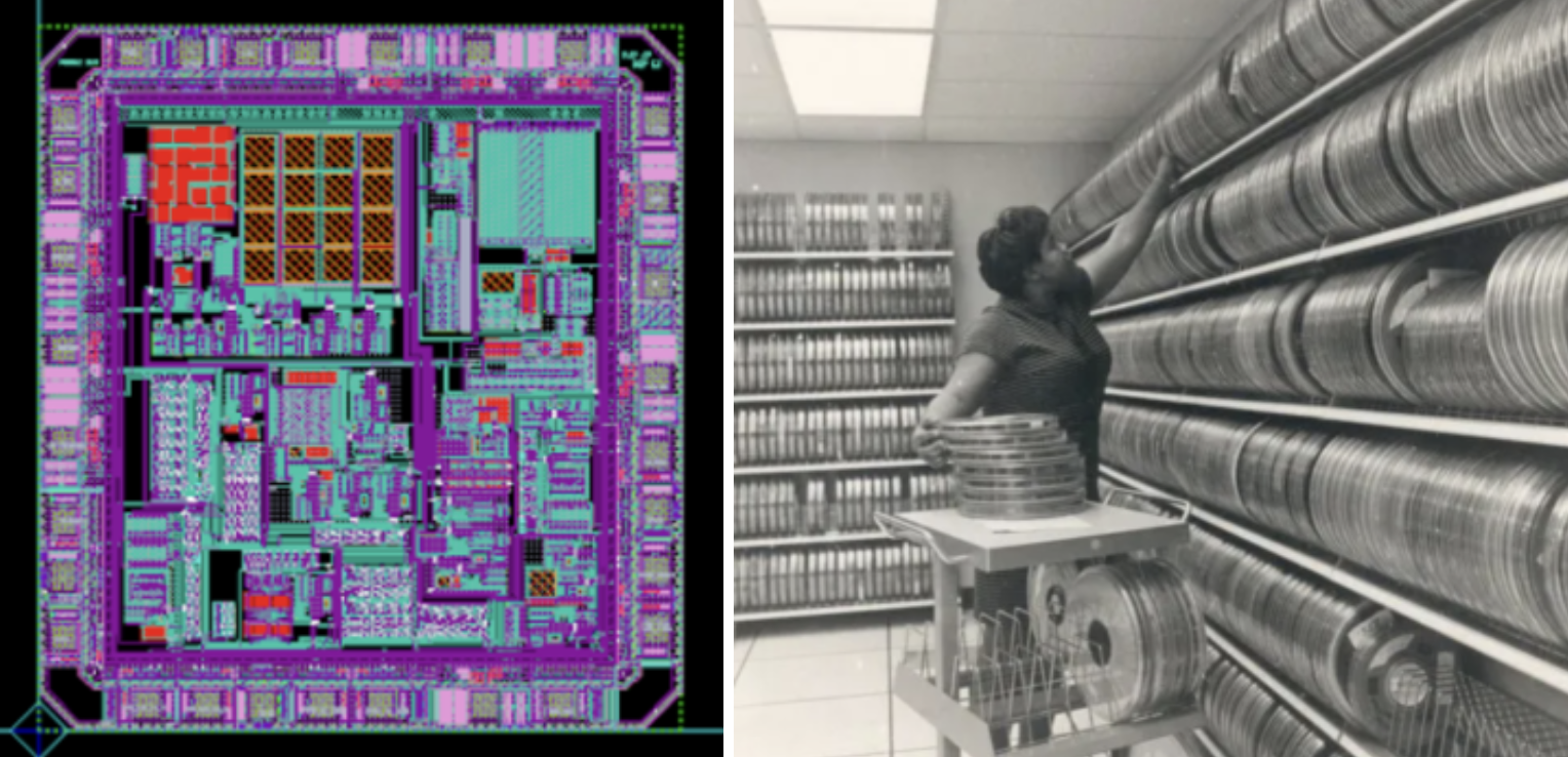
A single error in the tape could ruin a chip, and delivery delays were a constant worry. Today, tape-out is a digital process, with GDSII or OASIS files securely transferred to foundries like TSMC.
Yet, the stakes are higher than ever. At 2nm, designs pack billions of transistors, and the complexity demands flawless execution. TSMC’s N2 process, set for mass production in Q2 2025, uses nanosheet-based GAA transistors, pushing the boundaries of what tape-out must achieve (TSMC 2nm).
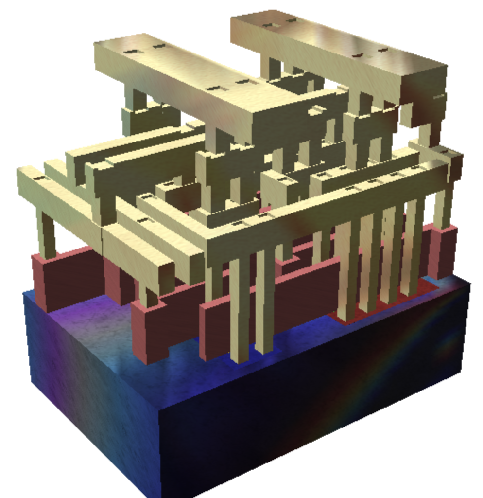
The Tape-Out Process: A Gauntlet of Precision
Tape-out is the final checkpoint before manufacturing, where the design team ensures the chip is functionally correct and manufacturable. The process is a gauntlet of verification steps, each critical to avoiding the dreaded re-spin. Here’s how it unfolds:
| Stage | Description | Key Tools |
|---|---|---|
| Functional Verification | Simulates the design to ensure logical correctness using millions of test cases. SystemVerilog and UVM drive this process, often supplemented by emulation platforms like Cadence Palladium. | Synopsys VCS, Cadence Xcelium |
| Static Timing Analysis (STA) | Verifies timing constraints to ensure signals propagate correctly within clock cycles. Identifies critical paths and timing violations. | Synopsys PrimeTime |
| Physical Verification (PV) | Includes Design Rule Checking (DRC) to ensure compliance with foundry rules and Layout Versus Schematic (LVS) to confirm the physical layout matches the schematic. | Mentor Calibre, Synopsys IC Validator |
| Power & Signal Integrity | Analyzes electromigration, IR drop, and thermal effects to ensure reliability, especially critical at 2nm. | Ansys RedHawk |
The sign-off moment is electric—when STA and PV teams report clean results, and the design is locked. For many engineers, it’s a rare chance to celebrate before the anxiety of awaiting first silicon kicks in (Tape-out).
The Stakes: Re-Spins and Market Pressure
Tape-out is a make-or-break moment. A successful tape-out sets the stage for production, but a flaw can trigger a silicon re-spin, where the design must be fixed and re-manufactured.

Re-spins are costly—$10M-$100M for a 5nm chip—and can delay market entry by 6-18 months, potentially ceding ground to competitors. A 2025 Wilson Research/Siemens survey reports that first-time silicon success rates have plummeted from 24% to 14%, with 75% of designs now behind schedule (Tape-Out Failures).
Why? The surge in AI-driven chip demand, coupled with design complexity, is stretching teams to their limits. Smaller designs (<5M gates) are surprisingly more prone to re-spins due to limited verification resources, underscoring the need for rigorous processes.
The Human Edge: Why Experience Matters
No tool can replace a seasoned engineer’s intuition. Those who’ve led multiple tape-outs know how to spot potential issues, from subtle timing violations to process-specific quirks. “Customer-centric tape-out strategies bridge market needs and technical precision” (TSMC Symposium).
Your experience—honed over years of debugging, optimizing, and navigating foundry requirements—is what ensures a design survives the tape-out crucible.

Until every violation is resolved, engineers live by the clock of EDA tool runtimes, often working through weekends, early mornings, and even sacrificing holidays.
Tape-out is more than technical—it’s emotional. The moment when Signoff teams declare “No violations!” is a rush, often followed by a team celebration or a brief respite before post-silicon validation begins. But the wait for first silicon is nerve-wracking, as any flaw could mean starting over. This blend /
of triumph and tension makes tape-out a defining experience for engineers, a badge of honor in your career.
Key Citations
- Tape-Out Failures Are The Tip Of The Iceberg
- 2 nm process - Wikipedia
- Challenges And Outlook Of ATE Testing For 2nm SoCs
- Scaling AI in the sector that enables it: Lessons for semiconductor-device makers
- Synopsys DSO.ai
- Siemens unveils AI-enhanced EDA tools
- TSMC 2nm Technology
- Tapeout Origin
- Tape-out Wikipedia
- TSMC Tech Symposium 2025