
Executive Summary
- Small Market and High R&D Burden: The EDA industry is a niche market with an extremely limited customer base, making research and development (R&D) for software development extremely costly.
- The limited number of chip design companies in the world makes it difficult to achieve economies of scale, resulting in high tool costs per individual customer.
- Because of the high cost of failure in advanced semiconductor design, chipmakers pay a premium for reliable tools with a high number of success stories (golden references), and EDA companies spend a lot of money to ensure tool accuracy and coverage.
- Foundries like TSMC and Samsung deploy methodologies for only officially certified EDA tools in their latest processes, and Fabless are tied to those tools, making it difficult to choose alternatives.
Structural causes for high prices
- Extremely small market size, R&D amortization, Duopoly:
- EDA is a very small market with its main customers being semiconductor design companies worldwide.
- There are many different stages of semiconductor design, and at each stage, not all three companies compete, but only two companies compete, creating a duopoly.
- With such a limited customer base, EDA companies must reinvest more than 30% of their revenues in R&D, while recovering development costs from a small number of customers. With a much smaller customer base compared to other industrial software, EDA companies can't lower prices by increasing sales volume.
- This results in a higher per-customer share of R&D costs, which makes it difficult to offer software as cheaply as traditional SaaS.
- This is the fundamental reason why a "free" or premium model can't take hold. This market structure is also the reason why EDA companies seek to recoup their R&D investments by continually raising prices rather than reducing them every year.
Duopoly 독점이면, you can charge more, right?
This is a one-shot perspective, and the EDA Industry is a repeated game + whales market, so it's not that simple.
Even if you have a monopoly, you don't have unlimited pricing power. The optimal solution for EDA vendors is usually not a "raise price N times" shock, but rather a combination of (1) annual uplifts + (2) creating a value proposition with new nodes/features/modules + (3) price discrimination by customer with ELAs to maximize long-term LTV.
- Buyer power is very high (fewer customers = more bargaining power)
Even if A_Product is the "golden reference", actual purchases are usually negotiated per ELA (Enterprise License Agreement)-Bundle-Credit-token, not per individual tool. Doubling the price does not double the "realized price". Rather, the customer cuts even harder in the next renewal. - Excessive price increases trigger "counter-investment" (grow substitutes)
Customers grow "long-term substitutes" such as expanding 2nd source, in-house tools, open source/research community, co-development with competitors in the next quarter/year, even if it is difficult to substitute immediately. Since EDA is typically a high maintenance (R&D) + network effects industry, the cumulative effect of these responses breaks the vendor's long-term profitability. - The headwinds are high because it's an "ASIC total solution" war, not an "ASIC step solution" war
If you overpay for A_Product, the customer will retaliate with bundle swaps in other areas (Implementation, Verification, DFT, etc.). In the end, you're trying to change the configuration while maintaining the total spend. Portfolio LTV is more important to the Product Manager: - Budget constraints + reduced seats/usage leads to lower "penetration"
If you raise the price, customers cry and eat mustard, and instead of "staying the same", they cut back on usage (reduced seats, limited runtime, only use at project gate), just like the demand/supply curve. This slows down standardization/diffusion, and in the long run, ecosystem dominance." - Foundry/partner ecosystems are "relationship assets," so the cost of breaking trust is high
At advanced nodes, EDA needs to co-optimize with customers/foundries/partners. Pushing too hard on price hurts non-price assets like collaborative data/early access/co-debugging. This is often more devastating than revenue." - Regulatory/reputational risk is also a real constraint
"De facto standard" The more extreme the position, the more legal/regulatory/PR costs are attached to pricing that looks like blatant extortion. PMs look at risk-adjusted returns, not just revenue.
If Commercial EDA Tools are expensive, why use them?
- High cost of failure and signoff risk:
- The value of an EDA tool is not just in the functionality it provides, but in the assurance of the final conformance of the chip design.
- In advanced processes, a single design mistake translates to tens to hundreds of millions of dollars in lost wafers and opportunities, so chip designers perceive the cost of failure to be far greater than the cost of the tool.
- There is a conservative culture in the semiconductor industry that is intolerant of failure, with industry wisdom stating that "if a chip fails, the financial and opportunity costs are enormous."
- As a result, design teams try to reduce risk by transferring some verification responsibilities to EDA tools.
- It's as if the tool is acting as a kind of insurance, and the customer pays a premium for this safeguard.
- Tool vendors also go to great lengths to ensure that the chips taped out through their tools are free of problems, and this liability of verification is ultimately reflected in the cost of tool development and support, resulting in higher prices.
- In short, the price of EDA tools includes the cost of the right not to fail, and this structure makes it difficult to apply a low-cost or free model like general software.
- Lock-in effect due to the foundry tie-in.
- The more advanced the node, the more essential it is for EDA tools and semiconductor foundries to collaborate, creating a dual ecosystem lock-in effect.
- Foundries collaborate with a handful of EDA companies such as Synopsys, Cadence, Siemens, and others from the process development stage to jointly develop PDKs (Process Design Kits), design rules, and models optimized for their processes.
- For example, TSMC, through its "EDA Alliance" program, certifies only select tools for the latest processes, such as 3nm, and even Siemens EDA has a high threshold that prevents some tools from being certified for 3nm.
- Foundries and fablesses accumulate a tremendous amount of design/process data every year and continue to propose improvements to existing EDA tools to EDA companies, who then develop the features with patents and distribute the methodologies to their customers.
- In this process-EDA nexus, it is almost impossible for new players to get the same certifications, and design teams have no choice but to use uncertified tools or risk manufacturing defects.
- In practice, advanced process designers only use tools that are officially supported by the foundry, given the multi-million dollar cost of masks, and low-cost, uncertified tools are not adopted due to high risk.
- As a result, stronger foundry-EDA cooperation and interdependence acts as a barrier to entry for market entrants and gives incumbent EDA companies a structural advantage to maintain high prices without competition.
- Once you've learned a tool, once you've created an environment, it's hard to move to another tool:
- Semiconductor design flows are based on decades of complex tool linkages and automation scripts, and it's costly and time-consuming to change the tool chain once built.
- In the past, a combination of "best in class" tools for each stage was sometimes used, but with the significant increase in the complexity and continuity of today's chip designs, compatibility and integration between EDA tools has become a major challenge.
- In response, the top EDA companies have tightly integrated and co-optimized their tools to provide platforms that cover the entire design flow.
- When a comprehensive solution from one vendor is adopted, replacing one individual tool with a third-party product has significant path dependency costs, including modifying associated scripts, converting design data, and retraining engineers.
- For example, a team using Synopsys' Logic Synthesis and Static Timing Analysis tools would need to switch to Cadence's tools. It takes months of effort to ensure that all current flows are compatible, that all current files are compatible, and that verification procedures are revisited.
- These S switching costs make customers reluctant to move away from their existing tools, and EDA companies can use customer lock-in to drive up prices.
- What's more, most EDA licenses are subscription-based, with a strong tendency to lock in a contract, and some large customers will even sign multi-year enterprise-wide license (ELA) agreements to reduce the likelihood of switching to another vendor.
- These high switching barriers make it difficult to penetrate the market through low price competition, and are a factor in the structural maintenance of the existing pricing structure.
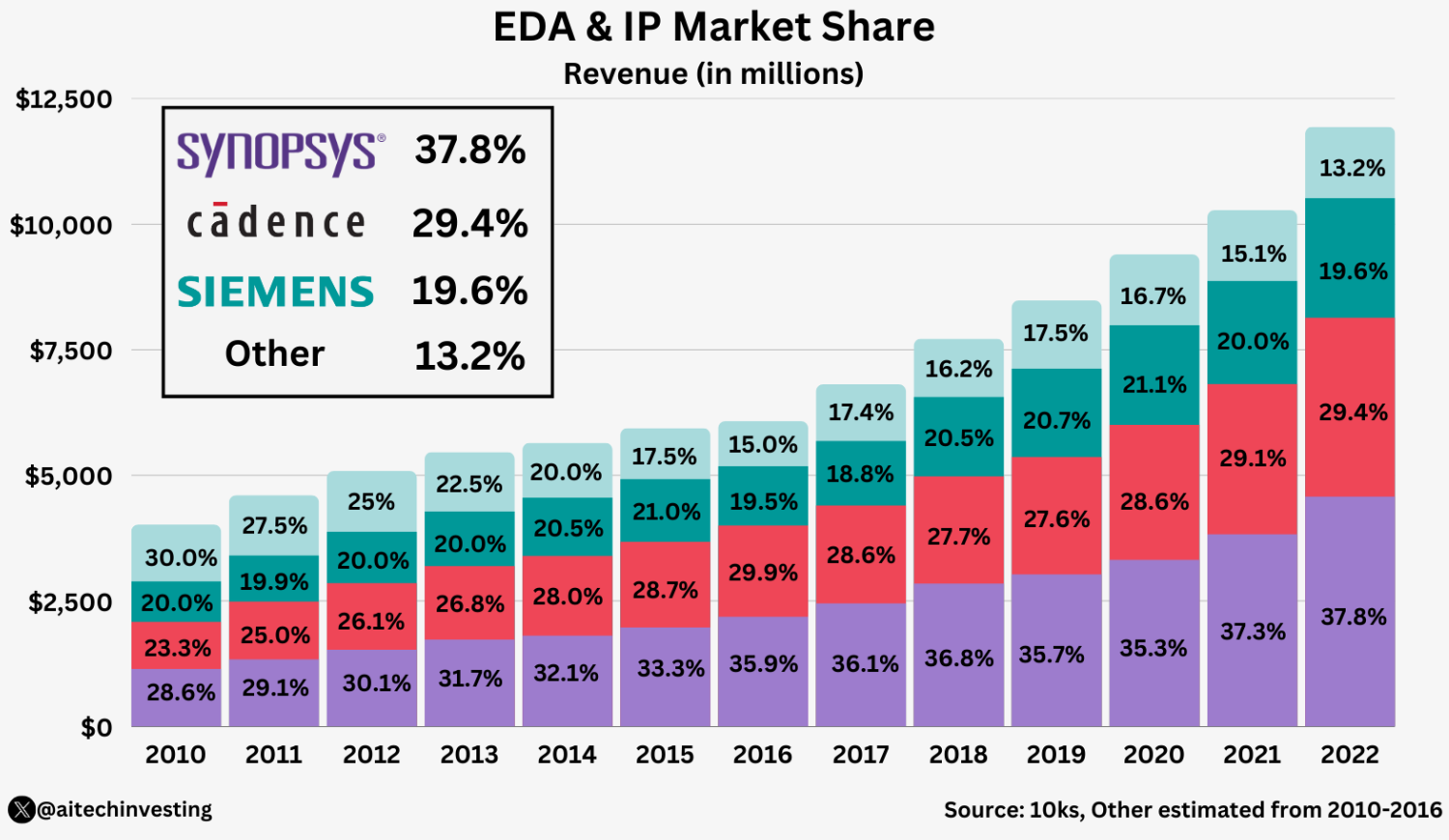
- Oligopoly and lack of competition:
- The current EDA market is effectively a Big-3 oligopoly, with Synopsys and Cadence alone accounting for more than 60% of global revenue.
- This structure is characterized by typical market failure: a small number of suppliers dominate the market, which limits price competition and allows for stable high pricing that borders on collusion.
- On the other hand, technologically superior EDA startups have emerged in the past, but most of them have been absorbed by mergers and acquisitions without ever becoming independent companies.
- For example, Xoomsys for parallel SPICE simulation, Extreme DA for multicore STA tools, and Rocketick for GPU-accelerated simulation were all acquired by Synopsys or Cadence for hundreds of millions of dollars despite their innovations, and all that was left was technology that was integrated into the larger companies' product offerings.
- The absence of independent new competitors soon solidified the pricing power of the incumbents.
- In addition, the EDA space is highly patent-locked, with decades of patents on core algorithms that put new players at risk of legal action if they develop similar functionality.
- Large players have used their extensive patent portfolios and deep pockets to block or acquire potential competitors from entering the market.
- Semiconductor design firms also prefer to work with large, proven players, making it difficult for smaller players to stand a chance.
- The combination of barriers to entry and lack of competition has resulted in EDA tool prices remaining high with little consumer pressure, unlike the traditional software market.
The EDA tool market has become a hard environment for low-cost models to take hold.
Core customers are more willing to pay for solutions with stability and support, even at higher prices. This is because EDA is more of a service than a functional product, selling trust and results, and we explore these misconceptions and future prospects in more detail below.
Rebuttal to the "EDA is prohibitively expensive" argument
One of the common complaints about EDA tools is "why is it so expensive for the same software?".
On the surface, annual licenses from Synopsys or Cadence can cost hundreds of millions to billions of dollars, which can make a layperson feel like there's a "pricing bubble."
But here's the real context:
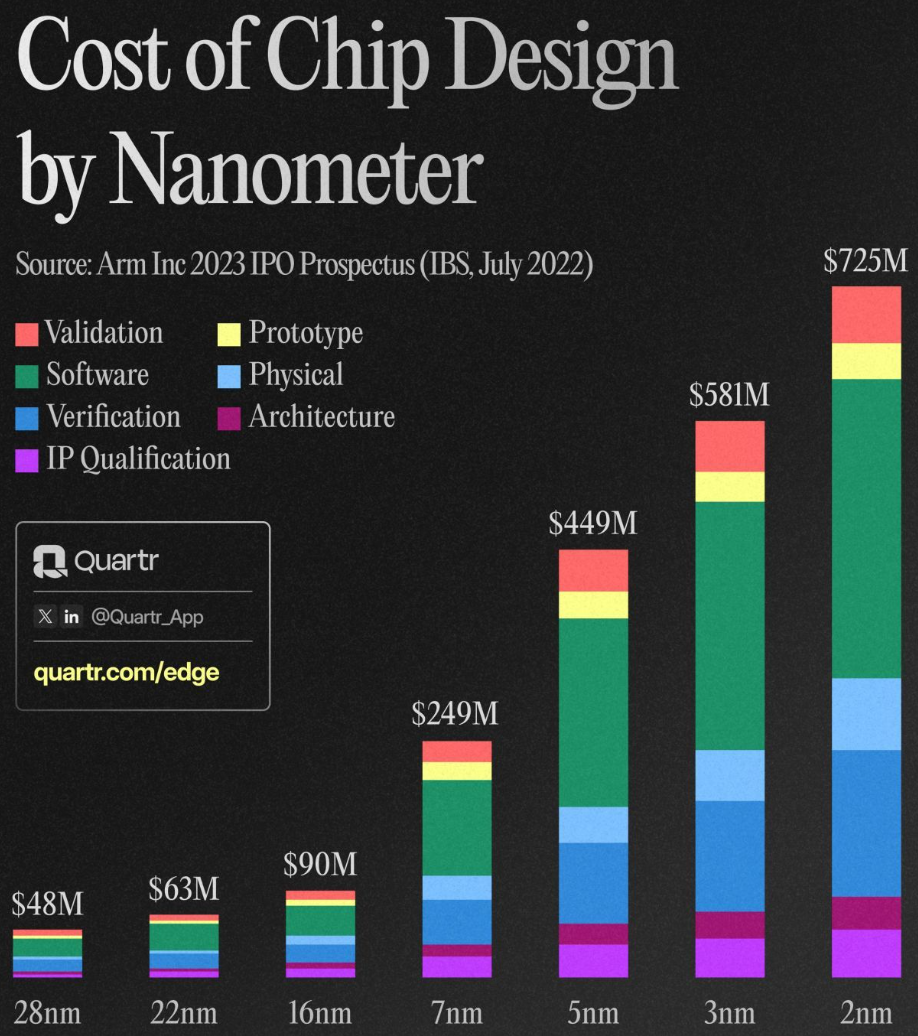
The value for money of EDA tools needs to be viewed in the context of chip design as a whole. The design cost of a leading-edge SoC can be as high as $650M on a modern 3nm process. [Reference: https://semiengineering.com/making-chips-at-3nm-and-beyond/#:~:text=Needless%20to%20say%2C%20the%20design,much%20a%20chip%20will%20cost]
EDA tools are only a small part of the total development cost, and other factors such as labor, IP licensing, and prototyping are huge.
In other words, EDA tools may seem expensive, but they save even more money by avoiding chip failures and reducing development time. Without a well-established tool chain, design would be impossible, or development manpower and time would grow exponentially, so the tool bang for the buck is huge.
This is why large semiconductor companies are willing to sign multi-million dollar multi-year contracts, as they are considered a investment that is essential to product success.
In addition, the EDA cost per unit of performance has been falling rather steadily.
As the number of transistors per chip has grown exponentially according to Moore's Law, EDA companies' revenues have grown, but the rate of growth has been limited, with design cost per transistor declining at more than 30% per year.
EDA tool vendors seem to be raising prices every year, but the design productivity gained by customers has more than made up for it, so "bang for the buck" is improving over the long term.
Indeed, the size of circuits that can be designed by the same number of people has grown exponentially over the past few decades, largely due to advances in EDA tools. So rather than judging a tool by its absolute price, you should consider the value it adds and how efficient it is compared to alternatives.
The high price of EDA is a structural necessity
- EDA companies also reinvest a significant portion of their revenue in R&D and customer support;D and customer support, and they have to support new processes and improve algorithms every year.
- If they were to cut their prices in half, it would be difficult to maintain the current level of technical support and updates, which would lead to decreased tool reliability and increased customer risk.
- Already, there is a saying in the industry that "EDA vendors never lower their prices," but this is more a result of responding to the growing complexity of tools and support needs rather than price fixing.
- As chip design complexity increases, so does the responsibility and burden on EDA tool developers, and pricing reflects this reality.
Finally, the "EDA tools are too expensive" argument ignores the uniqueness of the semiconductor industry. EDA tools are not like office software or general SaaS, where the same product is distributed to a broad user base; they are more like mission-critical tools that are responsible for the lives of a few customers.
In this context, EDA pricing is not just about software features, but about services that increase the probability of chip success. Therefore, it is not appropriate to criticize the price tag alone as "expensive," but rather to evaluate the value and risk savings that the tool provides.
Conclusion
The seemingly high and rigid pricing of EDA tools compared to general software is not a product of corporate greed, but rather an industry structural necessity.
In the B2B niche market, where a small number of customers demand a high level of reliability and support, EDA companies have responded by increasing value rather than lowering prices.
Dramatic price reductions are unlikely under the current structure. As long as foundry-EDA coordination, high switching costs, and oligopolies remain in place, EDA tools are likely to remain highly specialized products. However, there are conditions that could lead to a significant price decline.
For example, if open-source EDA becomes viable in certain areas with government and community support, or if a model emerges where foundries subsidize EDA costs to expand their chip design ecosystem, we could see some change.
It's also possible that AI could lead to a "two-tier market," where certain designs are automated and solved by "standardized, low- to mid-range tools," and only advanced custom design and final verification is left to premium tools.
But this transformation will take time and trust to materialize, and in 2025, the EDA market is still characterized by high barriers to entry and concentration.
In the end, fabless and foundry managers will have to play their best game with the status quo, while also looking for ways to increase the efficiency of using EDA tools through open innovation and collaboration in the long term.