VLSI Korea
Daily Silicon: GDI Jumps 13.2% as Photonic Computing Pushes Toward Deployment
🆓 무료 글 · 누구나 무료로 읽을 수 있는 글입니다 A practicing semiconductor engineer's daily read on global silicon news: Semiconductor prices lifted Korea's real GDI 13.2%, while new EUV and photonic-computing results shifted the question from lab performance to deployability. Read this every morning at 06:00 KST. Daily Silicon is VLSI Korea’s engineer-


🆓 무료 글 · 누구나 무료로 읽을 수 있는 글입니다
A practicing semiconductor engineer's daily read on global silicon news:
Semiconductor prices lifted Korea's real GDI 13.2%, while new EUV and photonic-computing results shifted the question from lab performance to deployability.
Chase's Take - I read the 13.2% GDI gain as a measure of Korea's domestic capture rate, not proof that the semiconductor upcycle is complete. The 9.4 percentage-point gap versus real GDP warns that better pricing and terms of trade do not translate one-for-one into production and employment.
In backend operations, domestic wafer starts, packaging slots, burn-in throughput and equipment localization expose the transmission path better than export value does. Likewise, 528 Gb/s/mm² is not deployable photonic compute density until microring thermal drift, calibration duty cycle, PDK variation and test cost are closed.
1. Why This Terms-of-Trade Gain Is Different: GDI 13.2% and Chip Prices
TL;DR - The Bank of Korea found that real GDI rose 13.2% YoY in Q1 2026 while real GDP increased 3.8%.
Higher semiconductor export prices, not lower imported oil prices, drove the improvement and made memory pricing and export mix leading variables for domestic purchasing power.
Source: Bank of Korea - Why This Terms-of-Trade Gain Is Different: GDI 13.2% and Chip Prices
2. Mitsubishi Electric, Rohm and Toshiba Target September Power-Chip Deal
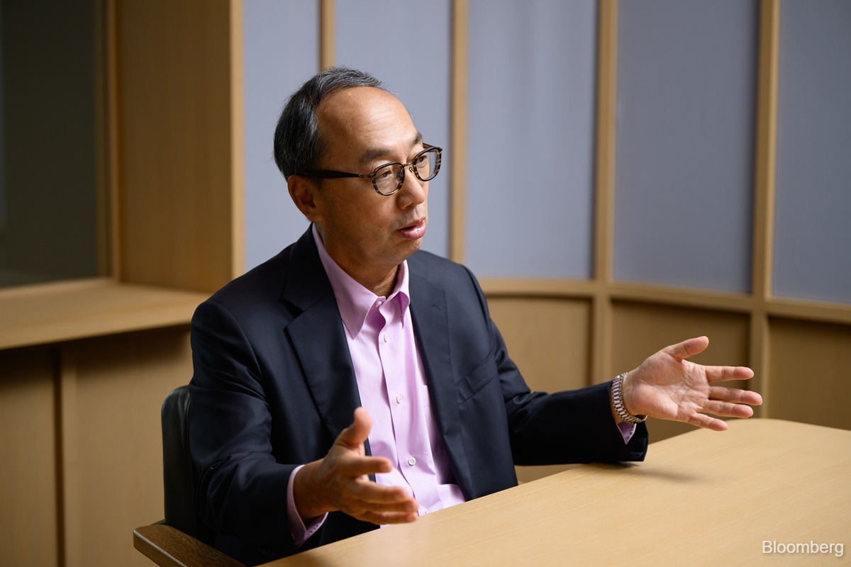
TL;DR - Mitsubishi Electric plans to announce an agreement by September to combine power-semiconductor sales, production and development with Rohm and Toshiba.
The first constraint is whether they can align product scope and governance as AI data-center power-conversion demand grows.
Source: The Edge Malaysia - Mitsubishi Electric, Rohm and Toshiba Target September Power-Chip Deal
3. 2 µm Laser-Driven EUV Source: Photons Take 70% of Input Energy

TL;DR - ARCNL reconstructed the energy partition of a 2 µm laser-driven tin LPP, with about 70% of input energy going to photons and 30% to plasma ions.
Source efficiency and collector lifetime require a closed photon-and-ion budget, not just 13.5 nm EUV output.
Source: Communications Physics - 2 µm Laser-Driven EUV Source: Photons Take 70% of Input Energy
4. Reconfigurable Photonic ALU Reaches 528 Gb/s/mm²

TL;DR - A silicon-microring photonic ALU reported 528 Gb/s/mm² compute density and 12.36 fJ/bit at 20 Gb/s.
Reconfiguring the same fabric for addition, subtraction and comparison moves photonic computing from a gate demo toward a programmable block.
Source: Nature Communications - Reconfigurable Photonic ALU Reaches 528 Gb/s/mm²
5. All-Optical RNN Beats the Linear Model Through 80 GHz
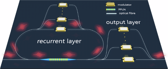
TL;DR - The all-optical RNN achieved 97.5% accuracy at 10 GHz, 92% at 50 GHz and 58% at 100 GHz on noisy-waveform classification, outperforming the linear model through 80 GHz.
Keeping linear operations, nonlinear activation and memory in the optical domain separates it from a basic optical matrix multiplier.
Source: Light: Science & Applications - All-Optical RNN Beats the Linear Model Through 80 GHz
6. Wavelength-Encoded Inference with MoS2 Photodetectors
TL;DR - A microcavity MoS2 photodetector array reached 99.6% on MNIST, 94.8% on CIFAR-10 and 94.0% on a spoken-digit dataset.
Integrating sensing, weighting and accumulation inside each pixel reduces data movement to external memory.
Source: Nature Communications - Wavelength-Encoded Inference with MoS2 Photodetectors
7. Cracking-Assisted Transfer Printing Produces 600 nm QD Pixels
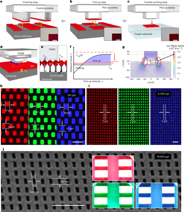
TL;DR - Controlled-cracking QD transfer printing produced 600 nm pixels with uniform patterning across areas up to 4 inch.
A cadmium-free full-color active-matrix display reached 1.41 inch, 320×360 pixels and 341 ppi.
Source: Nature Electronics - Cracking-Assisted Transfer Printing Produces 600 nm QD Pixels
8. Vapor-Deposited Perovskite Emitter Reaches 21.9% EQE

TL;DR - An X-type quasi-2D perovskite film from Seoul National University and Cambridge exceeded 85% PLQY, with PeLED EQE of 21.9% and a 16.8 nm emission linewidth.
The key result is thermodynamic control of the target crystal phase in an OLED-fab-compatible vacuum process.
Source: Tech Xplore - Vapor-Deposited Perovskite Emitter Reaches 21.9% EQE
9. Nanocrystal PN-Junction Model Explains QLED Ideality Factor of 42
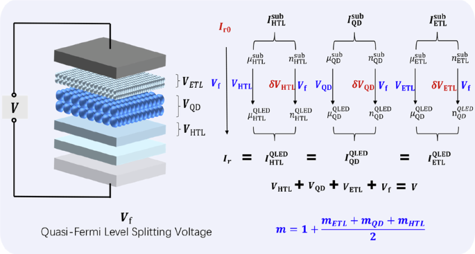
TL;DR - QLED ideality factors can exceed 20, versus 1-2 for conventional silicon PN junctions and 2-6 for GaN LEDs; a representative device measured about 42.
A model combining silicon PN-junction behavior with hopping transport explains the gap through layer-level voltage division.
Source: Light: Science & Applications - Nanocrystal PN-Junction Model Explains QLED Ideality Factor of 42
10. Thin-Film Modules Dock Mechanically and Electrically at 5-12 V
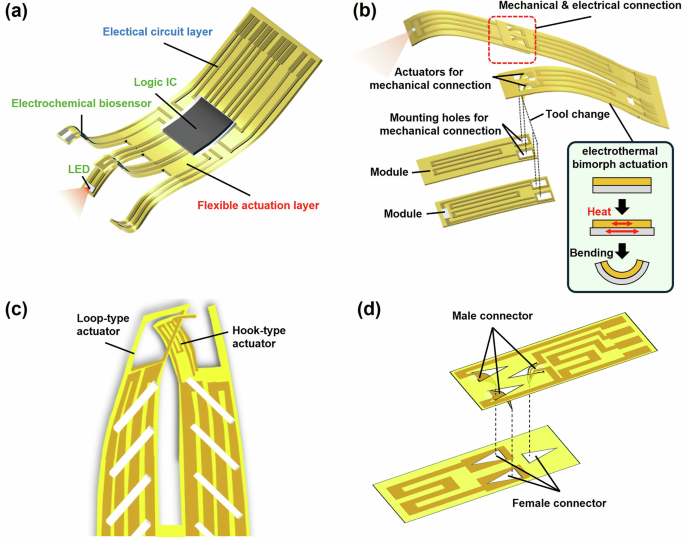
TL;DR - Thin electronic modules formed mechanical and electrical connections at 5-12 V and stayed coupled after power-off.
The probe produced 10 mm deformation at 1.1 W, while the detachable module averaged 0.43 W and 6.1 mN holding force.
Source: npj Flexible Electronics - Thin-Film Modules Dock Mechanically and Electrically at 5-12 V
11. Tin Oxide Replaces Indium in a 207.9 cm² Tandem Mini-Module

TL;DR - An indium-free perovskite-silicon tandem mini-module achieved certified efficiency of 31.0% over 207.9 cm².
Tin oxide costs about 1% as much as indium, while a 1 cm² cell reached roughly 33%, targeting material cost and area scaling together.
Source: Tech Xplore - Tin Oxide Replaces Indium in a 207.9 cm² Tandem Mini-Module
12. Intel-Powered Medical Exoskeleton Logs 40,000 Training Records
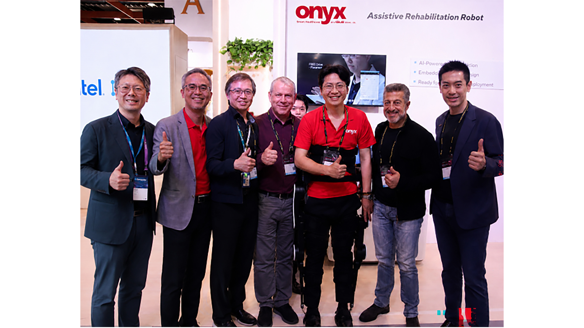
TL;DR - The FREE Walk exoskeleton uses Intel Core Ultra and OpenVINO to place local inference across the CPU, GPU and NPU, converting EMG, pressure and inertial signals into motion.
The platform has accumulated more than 40,000 patient training records across 22 countries.
Source: Intel - Intel-Powered Medical Exoskeleton Logs 40,000 Training Records
Daily Semiconductor Market Board
TradingView delayed quote basis. Click each ticker for the TradingView chart. Change uses daily change.
| Company | Ticker | Price | Daily Change |
|---|---|---|---|
| NVIDIA | NVDA | $204.71 | +0.94% |
| AMD | AMD | $508.57 | +2.58% |
| Broadcom | AVGO | $377.41 | +1.78% |
| TSMC ADR | TSM | $401.63 | +0.82% |
| ASML | ASML | $1,739.11 | -0.48% |
| Arm | ARM | $271.15 | +1.48% |
| Qualcomm | QCOM | $170.85 | -0.54% |
| Micron | MU | $868.72 | +2.33% |
| Intel | INTC | $97.46 | +2.55% |
| Applied Materials | AMAT | $534.34 | +0.88% |
| Lam Research | LRCX | $311.79 | -0.48% |
| KLA | KLAC | $212.54 | -0.10% |
| Samsung Electronics | 005930 | KRW 244,000 | -4.31% |
| SK hynix | 000660 | KRW 1,764,000 | -4.23% |
| Hanmi Semi | 042700 | KRW 222,000 | -8.45% |
What to Watch Next
- Semiconductor value and volume in Korea Customs Service's July 1-20 trade flash
This will show whether the Bank of Korea's price-led terms-of-trade gain is translating into export volume and domestic production. - Mitsubishi Electric, Rohm and Toshiba JV ownership, product scope and fab allocation in September
Customer qualification and process-transfer schedules will determine supply stability more than combining three sub-5% market shares. - 13.5 nm conversion, ion energy and collector contamination in 2 µm EUV LPP
Industrial viability requires calculating usable EUV dose from the 70% photon share alongside source lifetime. - Photonic ALU thermal drift, calibration duty cycle and cascaded bit error rate
The reported 528 Gb/s/mm² becomes deployable compute density only if it survives PDK corners and temperature variation. - KLA FY2026 Q4 results and process-control guidance on July 28
They will show whether added complexity from EUV, GAA and advanced packaging is converting into inspection and metrology revenue and customer utilization. - Teradyne Q2 results on July 28 and outlook call on July 29
These updates will expose how AI accelerator, HBM and automotive demand is affecting ATE utilization and burn-in capacity.
Other Semiconductor Headlines
- Nanophotonic SPRM Detects Weakened Single-Cell Adhesion Within 25 Seconds (Microsystems & Nanoengineering)
The 25-second detection and sub-nm uncertainty are strong, but the biomedical-sensing application sits outside today's semiconductor supply-chain focus. - Self-Powered Microfluidic-Optical Platform Detects 0.5 nM Thrombin in 5 Minutes (Microsystems & Nanoengineering)
The portable optical-sensor integration is promising, but clinical-matrix interference and a volume-production process remain open. - Hybrid Positioning System Combines GNSS with Fiber-Optic DAS (Tech Xplore)
It is relevant as a low-power edge workload, but accuracy and silicon-resource numbers were not disclosed. - Scheme Verifies Quantum-Computer Gates Without Access to Internal Structure (Phys.org)
This is a theoretical proof of device-independent certification; validation on a physical quantum processor is still pending. - Chip Industry Week in Review: Fab, EDA and Packaging Updates for July 17 (Semiconductor Engineering)
This roundup includes events already covered in recent Daily editions, so I did not repeat them as standalone items. - Samsung Vision AI Companion Adds Multi-Agent Support in 10 TV Languages (Samsung Newsroom Australia)
It confirms demand for on-device and cloud agents but provides no silicon specifications for NPU, memory or power budget.
Further Reading on VLSI Korea
- Die Shot Analysis ① Reading Floorplans from Intel 80486 to Sandy Bridge
Useful background for reading physical hierarchy, placement and implementation tradeoffs behind today's device claims. - The Kimi K3 Shock: Semiconductor Selloff, AI Chip Design and Apple
Connects AI-model shifts with chip-design economics and semiconductor market reactions. - After Graphcore: What AI Chip Startup Failures and M&A Reveal
Explains why benchmark performance alone does not close productization, software and capital constraints. - Furiosa, Rebellions and Chinese GPUs: Sovereign AI's Real Moat
Adds context on domestic value capture, supply-chain control and deployment economics. - From Hailo to Innatera: The Edge and Physical AI Chip Survival Map
Provides deployment context for edge inference, latency, power and workload-specific silicon.
Frequently Asked Questions
Why did Korea's real GDI rise 13.2% in Q1 2026?
The Bank of Korea found real GDI rose 13.2% year over year in Q1 2026 while real GDP increased 3.8%. Higher semiconductor export prices, not lower imported oil prices, drove the improvement.
What did the reconfigurable photonic ALU achieve?
A silicon-microring photonic ALU reported 528 Gb/s/mm² compute density and 12.36 fJ/bit at 20 Gb/s. Reconfiguring the same fabric for addition, subtraction and comparison moves photonic computing toward a programmable block.
How did the all-optical RNN perform?
The all-optical RNN achieved 97.5% accuracy at 10 GHz and 92% at 50 GHz on noisy-waveform classification, outperforming the linear model through 80 GHz. It keeps linear operations, nonlinear activation and memory in the optical domain.
What did the tin-oxide tandem mini-module achieve?
An indium-free perovskite-silicon tandem mini-module achieved certified efficiency of 31.0% over 207.9 cm², using tin oxide that costs about 1% as much as indium. A 1 cm² cell reached roughly 33%.
What power-chip combination is planned in Japan?
Mitsubishi Electric plans to announce an agreement by September to combine power-semiconductor sales, production and development with Rohm and Toshiba. The first constraint is aligning product scope and governance as AI data-center power demand grows.
Related reading
- Daily Silicon: Intel 18A, AI Silicon: 256 Cores, 16 Memory Channels
- Daily Silicon: Intel's $15B Offering: AI Silicon and Chip-Design Capex
- Daily Silicon: Intel at $16.1B: AI Chip Design and 18A
- Daily Silicon: Intel-Apple Chip Deal Surges 10%, Samsung-SK Cap Gap…
- Daily Silicon: Intel 18A-P Risk Production, SK Hynix Nasdaq ADR, TSMC…