
Semiconductors age too
Today's Semiconductor devices undergo a kind of "aging" phenomenon where their performance slowly degrades over time.
Just as mechanical parts wear out over time, MOSFET transistors change their electrical characteristics over long periods of operation, affecting the behavior of the circuit.
This phenomenon is called semiconductor aging, and the main causes are Bias Temperature Instability (BTI) and Hot Carrier Injection (HCI).
Aging causes the threshold voltage to increase, the drain current to decrease, and the switching speed and reliability of the device to degrade over time.
The end result is degraded circuit performance and reduced lifetime, which can lead to unexpected failures in the field.
In the early days, it was common to over-conservatively design circuits to prevent this aging, leaving a large margin of safety. However, with the ultra-micronized transistors of modern processes, we can no longer afford to give up performance by such a large margin.
Particularly in advanced nodes such as FinFET, GAA, process variations and thermal factors have increased further, making reducing unnecessary margins and achieving optimization through accurate aging prediction a key to competitiveness.
In the following, we will review the BTI and HCI mechanisms, their implementation in SPICE models, the use of time-based aging corners, and their industrial significance:
1. Semiconductor Aging Mechanism Conceptualization: BTI and HCI
Bias Temperature Instability (BTI) and Hot Carrier Injection (HCI) are two typical mechanisms of CMOS transistor aging.
https://m.blog.naver.com/gc_na/223392386850
Two key pillars of semiconductor aging: BTI vs HCI
1) BTI (Bias Temperature Instability)
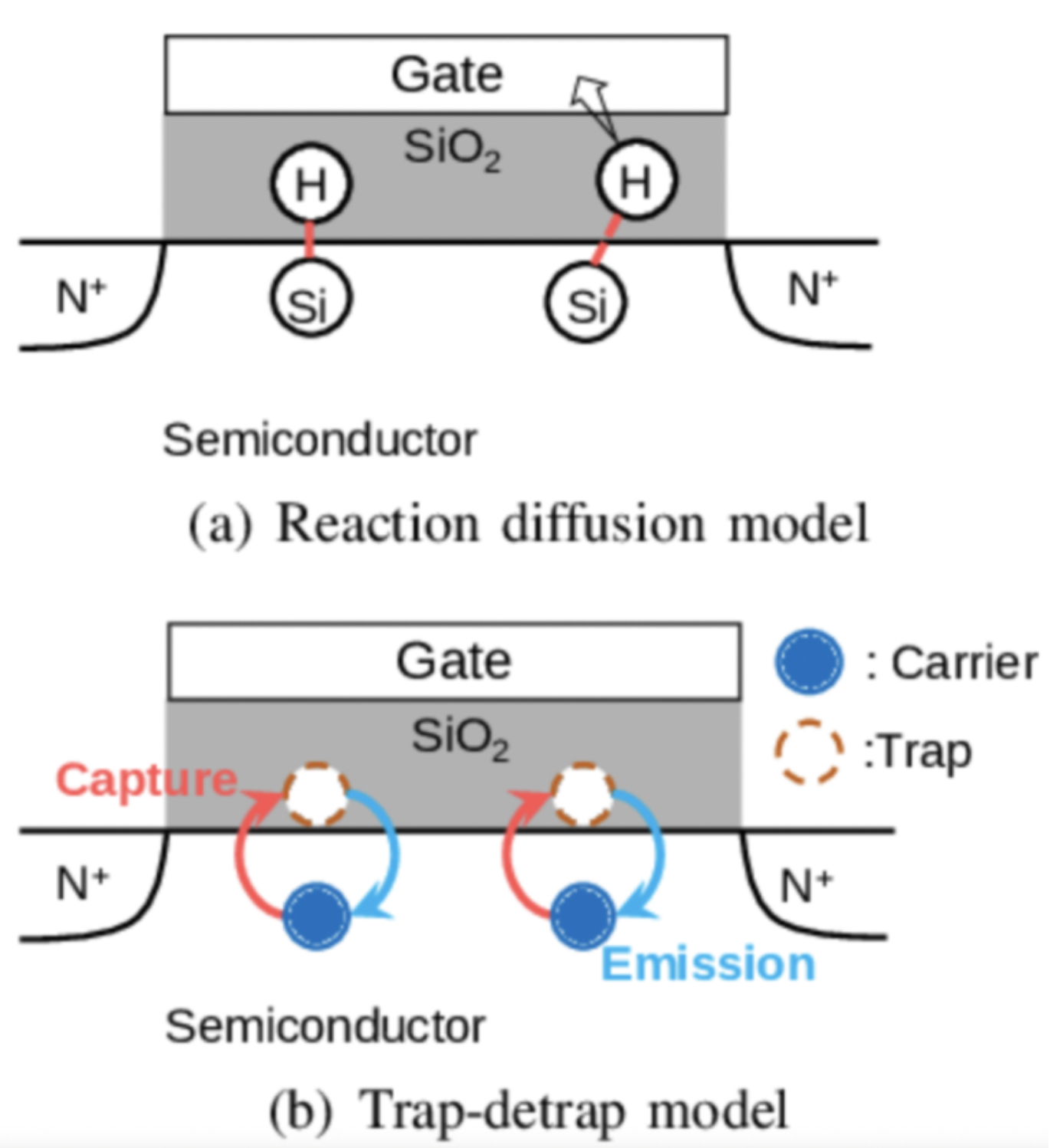
When the temperature rises to the temperature while the voltage is applied, Trap occurs between Gate Oxide and Channel → Threshold Voltage(Vth) increases
✔ What phenomenon?
- Negative BTI (NBTI)
- Positive BTI (PBTI)
✔ Result
- Vth increases, Drive current decreases
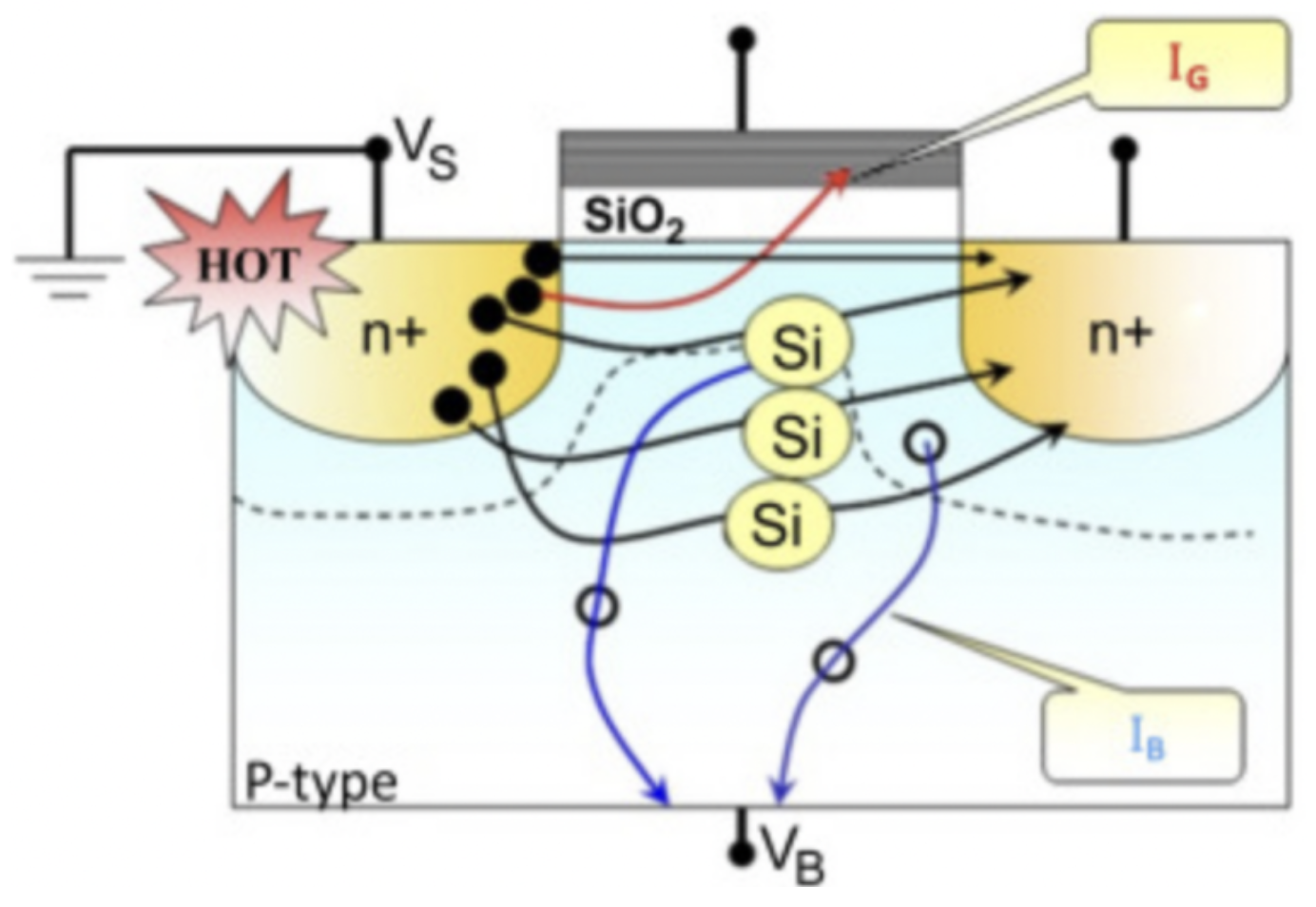
2) HCI (Hot Carrier Injection)
When the transistor signal is switched, high energy electrons (Hot carrier) jump out of the channel and impact the gate oxide → create a trap.
✔ Under what circumstances?
- High Vds + fast switching
- especially severe in NMOS
- NMOS HCI much more critical than PMOS
✔ Consequences
- Increased Vth, decreased drive current
HCI and BTI in action
1. HCI: "Very large electric field near the drain"
Taking NMOS as an example,
- If Vds is large and Vgs is also high enough,
there is a very strong electric field near the drain.
This electric field imparts extremely large kinetic energy (=hot carrier) to the electrons flowing along the channel.
2. Hot carrier "physically damages" the oxide/interface."
Hot carriers do two things:
(1) Break bonds at the Si-SiO₂ interface → Increase interface traps
When an electron strikes the oxide interface at a high energy state, the interface bonds are broken, increasing the interface trap density.
(2) Charge is mobilized inside the oxide film → oxide trap increases
Some hot carriers are injected into the oxide side, and positive/negative oxide charges are generated inside the oxide film.
In the end, interface trap increases → scattering increases → mobility decreases → I_dsat decreases.
Vth change (increase or decrease) due to HCI
Vth can be expressed as follows:
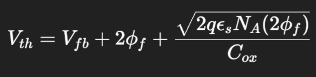
The Delta V_threshold due to the phenomenon of trapping charges is modeled as below.
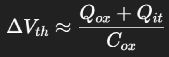
Here, depending on the polarity of the trap, V_th increases or decreases. (In general, electrons trap more than holes, so V_th often increases.)
⚡ BTI vs HCI at a glance
item | BTI | HCI |
Cause | Voltage + temperature stress | Fast switching + high Vds |
impact | Increase Vth → Increase Delay | Channel/Gate trap → Drive current decrease → Delay increase |
Mostly Occurs | PMOS(NBTI), NMOS(PBTI) | NMOS |
Temperature effects | as much as | Relatively small |
Supply voltage impact | as much as | Very Large |
In short, the more semiconductors are used, the more their physical properties change. BTI and HCI are typical phenomena.
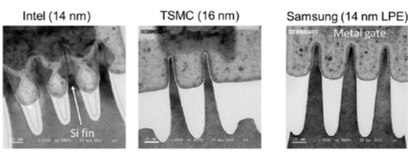
The nature of microprocess scaling and increasing aging severity
As the semiconductor node evolved from Planar → FinFET → GAA, device size reduction and thinning of gate dielectrics are making them more susceptible to degradation by BTI/HCI.
1) Gate Oxide is too thin: Dielectric at the level of a few atomic layers
- High-k/Metal Gates in modern nodes are a few atomic layers thick
- When this happens, the proportional impact of the charge impact (Qtrap) of a single trap increases exponentially.
- In other words, what used to be "one of hundreds of traps" at a node now acts more like "one of dozens" or "one of a few."
➡ Results: ΔVth, ΔIdsat changes cause much larger variation on a per-device basis.
2) Statistical Variation explodes due to smaller devices
As the device area gets smaller, the standard deviation of the Random Telegraph Noise (RTN / Trap Generation) distribution increases.
- Two transistors in the same process under the same stress conditions show completely different aging behavior
➡ Aging Variation itself becomes part of Timing Variation
3) Voltage Scaling Limit + Higher Temperature = BTI/HCI Acceleration
Due to high integration, the average temperature inside the chip has actually increased.
➡ The temperature stress on the chip goes up, so aging naturally becomes more severe
4) Process material changes create new aging issues
The introduction of High-k and Metal Gate, while beneficial for performance and gate leakage, has created new issues from an aging perspective.
- SiON → NBTI worsens (Nitrogen introduction effect)
- High-k (HfO₂) → severe PBTI occurs
➡ PBTI, NBTI issues worsen.
So, now we need to take this into consideration when designing circuits, right?
How to interpret SPICE
The PDKs provided by foundries today all include an Aging Model.
Standardization based on TSMC Modeling Interface (TMI) - CustomCMI API (CMI) - MOS Reliability Aging API (MOSRA) - Efficient Subckt Macro Modeling, Open Modeling Interface, etc.
- Foundry-provided BTI/HCI physics equations (ΔVth, μ degradation, etc.) are delivered in DLL form
- Circuit designers can use Spectre, AFS, HSPICE, etc. can call the same aging model regardless of which simulator they use
- Aging ΔVth, mobility reduction, etc. are reflected in SPICE parameters, so it is possible to reflect the actual I-V curve deformation as it is
BTI:
- Interface Trap vs Bulk Trap modeled separately
- Time exponent, Field-acceleration term included
- Recovery of AC stress is reflected as duty-cycle compensation
- Device size scaling (W/L dependence) added
The result is a complete time-voltage-temperature function for ΔVth(t, Vgs, T, duty).
HCI:
- Use an Impact Ionization Current (I_sub) or Lucky Electron based model.
- τ = A-(I_sub)^(-m)-exp(Ea/kT)
- Time-dependent interface state generation → ΔVth rises
- Mobility degradation is also taken into account
With the explosion of PBTI after the introduction of High-k, the model cannot be described by a single function.
As-grown + Generated (AG) BTI model and other models are being adopted.
Time-based model: End of Life
Chip design engineers usually give derates based on "End of Life (EOL)" or use libraries that are characterized for that derate. (In the case of SRAM, it is common to characterize the library according to the EOL and derate the cell.)
Nowadays, this derating method is not accurate, so there are methodologies such as Aging aware STA. (This is my specialty.)
https://semiwiki.com/eda/synopsys/312706-using-sta-with-aging-analysis-for-robust-ic-designs/
When aging models are included in SPICE, designers can do the following
1) Time-based Simulation
- Follow the voltage-temperature-duty cycle over which the transistor is actually operated
- SPICE integrates the time axis (stress history)
- At any desired point in time (e.g: 10 years)
- Interprets the circuit behavior again at the desired point in time (e.g., 10 years)
- E.g., HSPICE MOSRA's "One-step Aging" feature
2) Aging Corner Model
Foundry provides pre-aged SPICE model cards (e.g.: TT_125C_10Y)
Designer
- Fresh model
- Aged model (5 years, 10 years, etc.)
- Validates performance with all three versions.
Why is it important:
Specifically, the Automotive/Server/AP sector requires extreme mission profiles such as
- 10-15 years
- 125℃+
- 24/7 operation
- .
➡ Aging Corner validation is now a requirement for HPC/Flagship AP/Automotive.
5. Conclusion: Aging in the microprocessing era is not a 'choice' but a 'structural necessity'
As we move towards microprocessing, aging becomes explosively important for the following reasons.
- Gate stack thinning increases the impact of a single defect
- Device size reduction increases statistical variation
- Voltage scaling limits + thermal budget increases
- New materials (High-k) introduce new BTI/HCI issues
- Automotive/HPC market demands for longer lifetimes