
Let's take a deep dive into the inner workings of
FPGAs and ASICs
and explore the pros, cons, and business implications of both technologies.
- There are tons of semiconductor chips in our everyday lives, including smartphones, computers, and automotive electronics, but few of us really know the principles behind them.
- Electronic engineering students and embedded developers have often worked with FPGA boards, but they rarely have a detailed understanding of what the inner workings of an FPGA look like.
- Many have heard of ASICs but don't know exactly what they are.
We'll start with the layers of abstraction in semiconductor chip design, then move on to the structural differences between FPGAs and ASICs, a comparison of FPGAs vs ASICs from a technology, cost, and volume perspective, and some interesting questions like "Are GPUs and CPUs ASICs?".
Layers of abstraction in digital chip design
A complex digital chip design consists of several layers of abstraction. The highest level defines the behavior of the entire system, and the lowest level goes down to the atomic level of material phenomena. Here's a step-by-step breakdown:
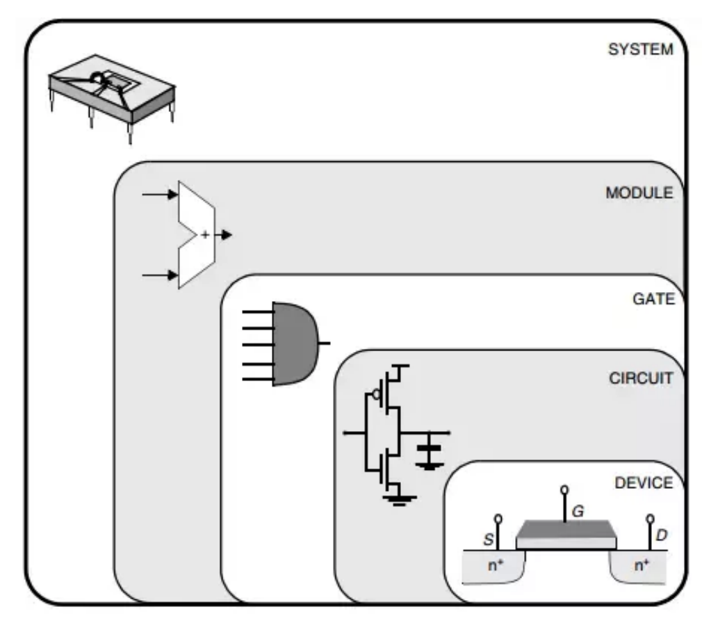
- System Level:
- Defines the functionality and behavior required at the product or system level.
- For example, designing the overall components and interfaces of a smartphone's communication modem, camera processing, AI computation, etc.
- Module Level:
- Design the major blocks (modules) that make up the system.
- Determine the internal structure (microarchitecture) of each functional module, such as CPU cores, memory controllers, DSP blocks, etc.
- Describe the behavior of each module in a hardware description language (HDL).
- Gate Level:
- Once the module design is complete, abstract it into a netlist of gates to implement it. Each function is implemented with a combination of logic gates, such as AND, OR, XOR, flip-flops, etc.
- The gates are represented by a predefined Standard Cell (ASIC) or LUT Combination (FPGA).
- Circuit Level:
- Each logic gate is ultimately implemented as a combination of transistors.
- For example, in a CMOS circuit, a NAND gate is composed of a few pMOS and nMOS transistors.
- At this stage, the behavior of the transistor schematic is often verified with SPICE simulation, for example[2].
- Device level:
- As a semiconductor device, transistors are driven by device physics, such as the field effect that moves electrons through the channel, and the process of depositing an oxide film and metal wiring on a doped silicon wafer.
- At this level, semiconductor process technology and device physics are important.
- Silicon level:
- At the most fundamental level, we can consider the crystal structure of doped silicon and the behavior of electrons at the atomic level.
- These physical phenomena are the fundamental basis for making the logic we design work.
This layer of abstraction, which goes from system → module → gate → transistor circuit → device process → material (atom), allows engineers to abstract away the detailed complexity at their design level.
For example, an RTL designer focuses on the functionality of the module rather than the gate or transistor, a Physical designer focuses on gate placement and wiring, and so on. With that background, let's take a look at how the inside of an FPGA and an ASIC, which are the two things we deal with most often, are organized:
Anatomy of an FPGA
- A Field Programmable Gate Array (FPGA) is a Programmable Chip that allows users to reconfigure the behavior of hardware in the field after manufacturing.
- "Gate Array", hence the name, has a grid-like arrangement of many programmable logic blocks inside, with a programmable wiring network connecting them.
- FPGA users design the desired digital circuit through HDL code, and then load configuration data called a bitstream into the FPGA to set the logic blocks' functions and wiring as desired.
-> As a result, FPGAs provide a hardware platform that allows for design changes and are widely used for rapid prototyping or low-volume production.
Let's take a look at the key elements one by one to understand the internal structure of an FPGA:
LUTs and flip-flops (Logic Cell)
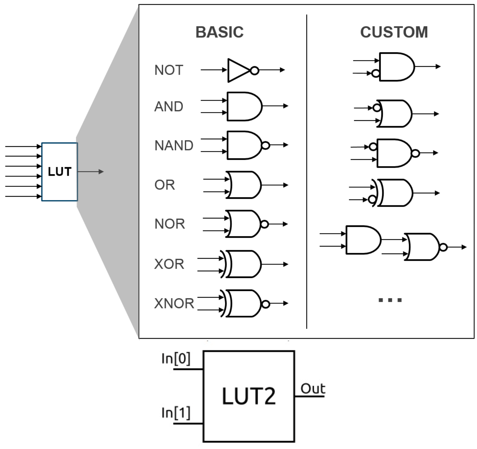
The basic building blocks of an FPGA are small logic cells.
Logic cells include lookup tables (LUTs) and flip-flops (FFs), and there are thousands to millions of these cells arranged throughout the FPGA.
LUTs are small memories that pre-table the output values for different combinations of inputs and are used to implement arbitrary combinational logic functions.
For example, a 4-input LUT would pre-store the output values for 4 bits of input in 16 memory cells, and output the values in those cells using the inputs as addresses. This way, even complex combinatorial logic expressions can be plugged into the LUT and achieve the desired result in a single cycle.
Most FPGAs use 4-, 5-, or 6-input LUTs, with a 6-input LUT storing the truth table in 64 SRAM cells.
A Flip flop is a 1-bit memory device that is connected to each LUT output and utilized as a register to implement sequential logic.
Typically, a single Configurable Logic Block or Logic Array Block in an FPGA is organized as a collection of logic cells containing multiple LUTs and flip-flops, for example, a CLB in a Xilinx FPGA is designed with two LUT+FF pairs in pairs, and so on.
LUTs can sometimes be chained together to act as larger LUTs, or they can switch modes, such as in combination with a small built-in full adder to perform simple addition functions.
Routing matrix and interconnect
Another key part of the FPGA is the programmable interconnect.
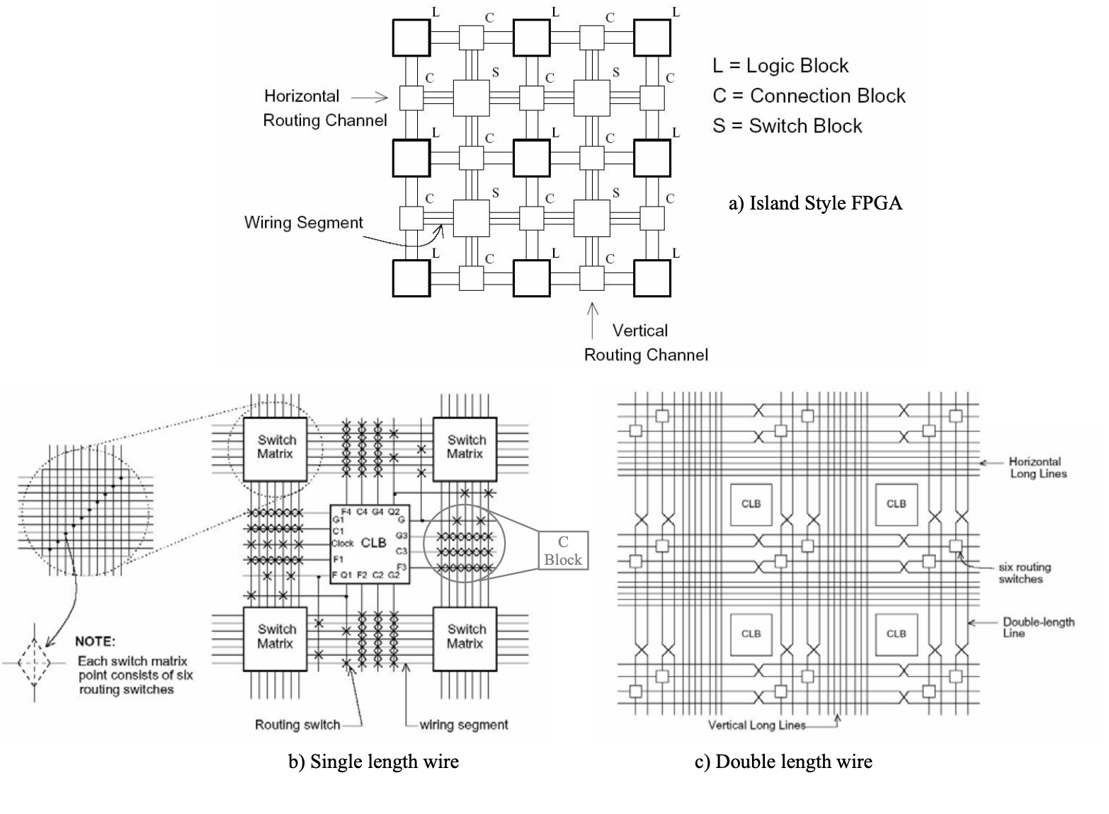
- To create the logic of a complex enough function to be a real product, you need to organize the wiring paths that carry signals to and from logic cells.
- In an FPGA chip, the inside of the chip is densely packed with wiring channels running horizontally and vertically, with switch matrices or routing switches at every intersection or branch point.
- These are a combination of programmable multiplexer/transistor switches that allow you to connect or disconnect any two signal lines you want.
For example, if you want to pass the output of one LUT to the input of another LUT a few rows away, you would turn the switches ON in the middle to create one continuous wiring path.routing resources are limited, FPGA vendors statistically optimize channel widths and switch counts to ensure that the design can be routed in most cases.
Each FPGA chip architecture has a different detailed routing structure (typically an "island style" structure), but conceptually, the entire wiring fabric can be thought of as acting like a giant switchboard.
Control information from this routing matrix is also embedded in the bitstream, which determines which logic cell outputs lead to which cell inputs by turning certain switches on and off.
In FPGAs, wiring delays and resource usage have a significant impact on performance, so Synthesis and place-and-route (P&R) tools automatically place LUTs to optimize LUT usage and wiring.
The more complex the circuit, the greater the demand for wiring channels as well as the number of LUTs, so ensuring that routing congestion does not become a performance bottleneck is key to FPGA design.
More recent FPGAs have introduced hierarchical routing, long-distance wiring (Line, Bus macros), and more to support a wider range of signal connections more efficiently.
I/O Pads
Along the edges of the FPGA chip are the I/O Blocks (IOBs) that send signals to and from the outside of the chip.
Each I/O block has an IO pad and associated buffers, transceivers, etc. that connect the FPGA's internal logic signals to external pins.
FPGA I/O blocks are programmable to support a variety of electrical standards, for example, you can set multiple I/O voltage and differential signal modes, including 3.3 V LVTTL, 1.8 V LVCMOS, LVDS, and PECL.
You can also flexibly configure I/O characteristics, such as adjusting the slew rate of output drivers, Schmitt triggering inputs, or embedding pull-up/pull-down resistors.
Higher-end FPGAs have high-speed transceivers (SERDES), PLLs for high-frequency clocks, oscillator drivers, etc. placed around the I/Os, allowing them to implement high-speed interfaces beyond simple GPIOs (e.g., PCIe, SATA, HDMI, etc.).
I/O blocks also have their mode of operation determined by the bitstreams that make up the FPGA.
Bitstream and configuration memory
So far, the logic blocks (LUT/FF) and routing of the FPGA, I/O, etc. have programmable switches, the set of information that sets these switches is called a bitstream.
The bitstream is a binary file of sorts, which is loaded into the configuration memory inside the FPGA. Most FPGAs use SRAM-based configuration memory, which means that the settings are lost when power is removed. Some FPGAs (e.g., those from Microsemi/Microchip) use flash or a semi-reversible antifuse method to maintain the configuration without power."
The bitstream is generated by the FPGA vendor's toolchain, which goes through HDL design → synthesis → implementation, and finally results in a bitstream file specific to that FPGA chip.FPGA behaves as the circuit you want.
The flexibility of FPGAs is that they can be reprogrammed by loading a new bitstream whenever needed. This flexibility is why FPGAs are widely used for prototyping, research and development, and low-volume production.
If you need to modify your design, you only need to put a new FPGA bitstream on the board, which is much more agile and economical than a silicon re-spin, which can take months and a lot of money.
정리: FPGA internal structure
(a) blocks of logic cells composed of multiple LUTs+FFs
(b) a network of programmable wiring connecting them
(c) I/O blocks supporting various interfaces
(d) bitstream memory that organizes them all.
This structure gives FPGAs the flexibility to implement a wide variety of digital circuits, but on the flip side, because they are designed to be general-purpose, they introduce a lot of unnecessary logic and wiring overhead when implementing a specific circuit.
This results in lower operating speeds and lower power efficiency than ASICs. The following ASICs are chips that have been optimized for specific functions by reducing this overhead to the extreme.
Internal structure of an ASIC
An application specific integrated circuit (ASIC) is a semiconductor chip that is custom designed for a specific use or application. Once manufactured, its internals can no longer be changed, and it only performs the functions defined in its design.
So how does an ASIC design and implement its internals? While it varies by size and design method, most modern ASICs use a standard cell-based design technique. Let's break down the internal structure and physical design elements of a standard cell-based ASIC:
Standard cell based design
A standard cell is literally a small logic circuit cell of a pre-standardized size. It is a grouping of transistors/wiring structures in a single cell that provide functionality as either an illogical gate such as an AND, OR, XOR, or inverter, or as a memory device such as a flip-flop or latch.
Each standard cell is internally composed of a number of MOSFET transistors, with the cell's input/output pins, power and ground pin locations defined.
All cells are designed so that their width varies by function, but their height is the same, so that when they are stacked horizontally, like Lego blocks, the power rail and the ground rail interlock in a straight line.
This means that when you place a standard cell horizontally in a chip design, the VDD wire at the top and the VSS wire at the bottom are straight, connecting to the entire chip power grid.
When designing an ASIC, the logic designer designs the circuit in HDL and uses a Synthesis tool to obtain a netlist of the standard cells needed to implement the circuit.
The result of the synthesis is a list of tens to hundreds of millions of cell instances and their connections, which specifies, for example, "500 AND cells, 200 OR cells, 100k flip-flops..." and so on, to realize the desired logic.
The Placement and Routing Tool (P&R) then takes this netlist as input and creates row after row of standard cells on the chip area and connects the inputs and outputs of each cell by routing them to each other.
Since standard cells are uniform in size, we stack them up in rows, and when these rows of cells are densely packed throughout the core area of the chip, we have the logic we want.
In addition to digital circuits composed of standard cells, an ASIC may contain specialized blocks such as memory macros (SRAM/ROM), analog circuits (PMICs, PLLs, etc., and I/O cells.
Since these blocks are not standard-cell sized, they are designed by placing them in the appropriate locations during the ASIC floorplanning phase and filling in the remaining space with rows of standard-cell logic.
For example, in an SoC ASIC, large blocks such as CPU cores, DSPs, on-chip memory, and IO physical layer (PHY) are placed first, and standard-cell logic fills in the remaining areas.
Standard cell libraries contain the physical layout, electrical characteristics, timing characteristics of each cell so that EDA tools can reference them to optimize the placement/wiring.
After creating a mask based on the finished layout to implement the circuit on the silicon wafer, the ASIC chip is born.ASIC's internal structure is a customized circuit made by assembling pre-designed standard cell components.
Whereas an FPGA builds everything with general-purpose logic blocks + routing, an ASIC implements only the functionality it needs into the circuit, so there is little waste of resources.
This translates to higher density, performance, and power efficiency. However, flexibility is sacrificed because the design must be completed from start to finish and manufactured in one step.
Power Grid and Clock Tree
With millions to billions of transistors running inside an ASIC chip, it is very important to provide a stable power supply to the whole thing and to deliver the same clock signal to all the flip-flops.PDN (Power Delivery Network) and the Clock Tree.
The Power Delivery Network is a network of metal wiring to provide enough power (VDD) and ground (GND) throughout the chip.
We mentioned earlier that when standard cells are placed in rows, each row has a single line of VDD/VSS wires, but this may not be enough to get power to the center of the chip.
So, the top metal layers form a lattice-like power grid that allows power lines to run across the chip.
Similar to the highways in a road network, the VDD/GND from the pads around the chip is distributed in an X/Y direction through the thicker metal layers, with vias to the lower metals in between to drop down to the standard cell power lines.
This allows power to be delivered from the edge to the center of the chip with minimal IR drop. Designing the power grid is an important part of the PDN design step, as is putting reinforcing metal around power-hungry blocks.
The Clock tree, on the other hand, is the wiring network that distributes the synchronization signal (clock) to all the flip-flops in the ASIC. It's called a clock tree because it's simply distributed in a tree shape, but it actually involves a lot of sophisticated buffer insertion and branch wiring adjustments to match the skew.
To get the clock to tens of millions of flip-flops at the same time, you need to make the delay more or less uniform across the clock path.distribution buffers from the clock source (such as a PLL) to each major block, and finally, near each flip-flop, local buffers to clean up the signal.
High-performance ASICs use an H-Tree with the clock lines alone on the top layer of metal, and branching down to the bottom.
The clock tree is the fastest-switching signal network on the chip, so its dynamic power consumption is also a big part of the equation, which is why CTS (Clock Tree Synthesis) optimization is key to reducing unnecessary load and minimizing latency when designing the tree.
While FPGAs already have a somewhat standardized power/clock distribution structure inside them, ASICs have to do the power planning and clock aggregation themselves instead of giving designers the freedom to arrange them as they see fit.
This allows ASICs to optimize power and clocks for chip size to maximize performance.
Routing and physical implementation
The routing of an ASIC contrasts with the programmable interconnects of an FPGA, Once implemented in silicon by photolithography, it is fixed wiring that cannot be changed.
P&R tools utilize multi-layer metallic wiring to connect the inputs and outputs of many standard cells, drawing the lines in the shortest path possible.
Wiring layers typically have separation of roles, with the lower metal layers being narrower and for short signals, thicker and for power/clock, and so on, and connections between layers via vias according to design rules.
When the final wiring is complete, it must pass a DRC/LSVS check, and a timing analysis is performed to verify that all paths meet the desired speeds.
This is something we do in FPGA design, but it's much more rigorous in ASICs because it's harder to modify once taped out.
After the ASIC is wired, additional tasks such as package I/O placement, power pad connections, and ESD protection circuitry are also done. In the end, an ASIC chip is finished and is a single, fixed hardware implementation that will never change.
To summarize the characteristics of the internal structure of an ASIC compared to an FPGA
- Optimized structure with no redundancy (standard cell/custom design)
- Efficient power/clock distribution to maintain high performance even at large scale operations
- Fixed wiring to minimize unnecessary delays, does what it was designed to do
- but cannot be modified once built, zero flexibility
These characteristics of ASICs give them a significant advantage over FPGAs in terms of performance, power, and area. In the next section, we'll compare FPGAs and ASICs directly from a technical and business perspective.
FPGA vs ASIC: Technology, cost, and mass-producibility comparison
FPGAs and ASICs have distinct advantages and disadvantages in many respects, due to their different origins and goals. Here's a comparison of the differences between the two approaches, focusing on the main ones:
- Performance and power efficiency: ASICs are faster to operate and consume less power because they design circuits directly for a specific purpose. They have no unnecessary logic elements and optimized wiring, so they achieve higher clock speeds and lower power than FPGAs when performing the same function[22]. FPGAs typically have one order of magnitude lower performance and higher power consumption than ASICs due to logic/wiring delays caused by LUTs, programmable switches, etc. As a rough example, an FPGA can have a maximum clock that is tens of MHz to hundreds of MHz lower than an ASIC and use many times more power to perform the same computation. Of course, modern FPGAs have embedded hard IP, such as DSP blocks and memory, to close the gap, but the overall efficiency advantage is clear for ASICs[18].
- Flexibility and development time: FPGAs are reprogrammable, which is their biggest strength. When you want to modify your design or change a feature, you can simply fix the HDL and put up a new bitstream. This greatly reduces development time, and it's a great way to create prototypes early in the project to try things out[24]. Also, once delivered to the customer, you can upgrade hardware features in the field, just like a firmware update. ASICs, on the other hand, can take anywhere from a few months to a year or two to design, verify, and manufacture, and once produced, hardware features cannot be changed[25]. If a bug is found along the way, the chip must be revised and remade, resulting in very long lead times. Therefore, FPGAs have an advantage in reacting quickly to changes in market needs, while ASICs must be implemented to near perfection in the early planning stages.
- NRE and unit cost: ASIC development has a significant NRE, including circuit design labor, EDA tool fees, and photomask fabrication costs. The cost of a set of masks can reach tens of billions of won for state-of-the-art processes, making it difficult to recoup the investment unless the volume is substantial[26]. By comparison, FPGAs have near-zero NRE costs because they use off-the-shelf chips. FPGAs have a high unit cost per chip; non-semiconductor consumers can expect to pay tens to hundreds of thousands of dollars for an FPGA chip, whereas ASICs can cost tens or even hundreds of dollars per chip in mass production[27]. In summary, FPGAs are cheaper in low volumes, and ASICs are overwhelmingly cheaper in high volumes. For example, if you need 100 pieces of specialized equipment, you don't need to make them as an ASIC, but if you need a chip for a smartphone that sells 100 million units, it's much more economical to spend the initial 10 billion to make it an ASIC.
- Mass production and reliability: Because FPGAs use semi-finished, commodity chips, it's important to get the same FPGAs in the supply chain when mass producing a product. ASICs, on the other hand, are chips that are made specifically for your product, so you only need to produce as many as you need. However, there can be yield issues, so you'll need to work to improve yield initially. In terms of reliability, FPGAs are a collection of proven IP, so there's less risk up front, while ASICs are newly designed, so the possibility of failure due to design flaws needs to be well managed. Therefore, a common strategy for small startups rather than large enterprises is to prototype with FPGAs, test the market, and then move to ASICs when they're confident. From an engineering perspective, it's also relatively safe to ASICize logic that's first verified in FPGAs. In fact, the "prototype with FPGAs → mass production with ASICs" step is considered the gold standard in many product development processes[28].
- Functional integration and more: ASICs can have multiple functions on a chip (SoC) or even analog/RF circuits, depending on the design goals. FPGAs are also called SoC FPGAs and can include ARM processors, but custom ASICs are much more flexible in terms of overall system integration. Another advantage of ASICs in terms of IP protection is that they are hardwired with complex circuits, making them relatively difficult to reverse engineer, which is advantageous for security[29].
As shown in this table, technical requirements and business context will determine whether you choose an FPGA or go with an ASIC:
Are GPUs and CPUs also ASICs?
One interesting question: Are processor chips like GPUs and CPUs ASICs?"
The answer is "in a broad sense, yes."
After all, a GPU or CPU is a dedicated integrated circuit for a specific purpose.
For example, NVIDIA's latest GPU is a dedicated architecture for graphics/AI applications, with tens of thousands of cores specialized for graphics and parallel computation, high-speed memory interfaces, and more.
This means that GPUs can also be called "ASICs for graphics and parallel computation" because they are application-specific compared to general-purpose CPUs.
Similarly, a CPU for a PC or smartphone is a general-purpose processor, but it is itself a custom-designed chip and is made using ASIC design techniques.
So, it's very natural for physical design engineers from NVIDIA to go to QTI, and for QTI RTL engineers to go to NVIDIA.
But in general, the industry doesn't refer to CPUs or GPUs as ASICs because they're very much general purpose programmable processors, and the term ASIC is used to refer to non-programmable chips that primarily perform specific applications.
For example, a Bitcoin miner ASIC or a autonomous driving AI acceleration ASIC, chips designed to focus on a single function are called ASICs.
To make the distinction a bit further:
CPU/GPU = general-purpose processor, ASIC = chip dedicated to a specific function is a linguistic habit, but technically, a CPU or GPU is also a broad category of ASIC because it is a custom-designed chip based on standard cells.
FPGA manufacturers also often refer to FPGAs as "programmable ASICs" because they logically behave like ASICs, except that they can be reconfigured multiple times.
The bottom line is that GPUs and CPUs are technically subcategories of ASICs, but in common parlance, they're called differently.
결론: The industry is headed toward ASICs
We've compared the internal structure and characteristics of FPGAs and ASICs, as well as their advantages and disadvantages. FPGAs have been a great tool for electronics students and engineers due to their flexibility and short development cycles, and they will continue to play an important role in prototyping and low-volume specialty applications.On the other hand, ASICs are the ultimate choice for large-scale industries due to their higher performance, efficiency, and cost advantages in mass production.
The SoCs in our everyday smartphones, CPUs/GPUs in our PCs, AI accelerator chips in our data centers, and ADAS chips in our cars are all ASICs with tens of billions of transistors.
Particularly with the recent AI boom, there has been an explosion of development of ASICs such as NPUs/TPUs to make deep learning computations that used to be handled by GPUs more efficient. This shows that the future of technology is shifting from general purpose processors to specialized ASIC accelerators.
FPGAs tend to shine in startups and research due to their easiness of development, but when a product becomes successful and is used by millions of people around the world, it tends to migrate to ASICs.unrivaled performance/cost competitiveness in their applications.
Today, there is talk of a high barrier to entry for ASIC development due to a shortage of semiconductor design talent, but at the same time, the increasing utilization of FPGAs through cloud FPGA services, high-level synthesis (HLS), and more is driving the rapid porting of proven designs to ASICs.
"The industry is going ASIC", meaning that it is the customized ASIC chip that ultimately delivers value to the masses of users.
Even innovations that started out as FPGAs will be implemented as ASICs as the market grows, achieving greater efficiencies and economies.ASIC-centric evolution toward higher performance, lower power, and lower cost.
The semiconductor industry's final direction will be toward ASICs.