
![[Digital design] Latch based Static Timing Analysis](https://storage.ghost.io/c/e0/1d/e01dab3f-8599-4f20-85b3-3b2507a10672/content/images/size/w1200/2025/06/-------------2025-06-15-073417.png)
소개
Latch-based design is used in digital semiconductor design.
| Cell | Transistor count |
|---|---|
| D Latch | 12~16 |
| D Flip-Flop | 18~32 |
Compared to Flip-Flop-based design, it offers the advantage of reduced transistor count, which impacts power and area. A key benefit of latches is timing flexibility through time borrowing. However, Flip-Flops are more commonly used because they operate only on clock edges, providing the following advantages:
- Robustness against glitches.
- Easier pipeline design.
- Simpler block boundary design.
Thus, if (1)~(3) can be effectively managed, latch-based analysis can gain traction in high-speed designs.
Part 1: Differences and Basic Concepts of Latch and Flip-Flop
Latch-based design offers advantages over Flip-Flop-based design, such as reduced die size and timing flexibility through time borrowing. However, the level-sensitive nature of latches complicates Static Timing Analysis (STA), particularly in hierarchical designs, where timing closure presents additional challenges.
Comparison of Latch and Flip-Flop Operation
- Latch: Level-triggered, becoming transparent when the enable signal is at the active level (high for positive-level latch, low for negative-level latch). Data passes from D input to Q output, and the last value is held when the enable signal is deactivated.
- Flip-Flop: Edge-triggered, capturing data on the rising or falling edge and holding it until the next edge.
Timing Analysis Basics
- Launch Latch: Begins launching data on the rising edge and continues until the falling edge.
- Capture Latch: Captures data based on the clock level.
- Waveform Analysis: For a positive-level latch, it becomes transparent when the clock is high, passing data, and holds data when the clock goes low.
Summary
To meet the setup time condition for a Flip-Flop, data must arrive before the clock edge.
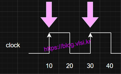
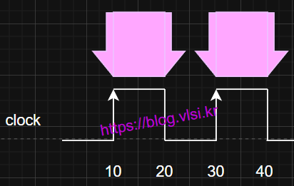
Latch requires data to arrive during the Clock's Enable.
Example: Three Latches Connected in Series
Consider a circuit with three sequential cells (L1, L2, L3) connected in series, controlled by the same clock.
- L1, L3: Flip-Flop
- L2: Latch
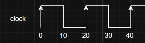
The clock period is 20ns with a 50% duty cycle.
- Clock is High from 0-10ns.
- Clock is Low from 10-20ns.
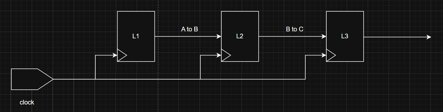
Data Propagation
At t = 0ns (Rising Edge): L1 becomes transparent, and L1’s D data propagates through combinational logic to L2’s D input.
- L1 → L2 delay: Assumed to be 24ns.
- L2 → L3 delay: Assumed to be 5ns.
- At 24ns, data is transferred from L1 to L2. Since the clock is High from 20-30ns, the latch receives the data without issues. (In a Flip-Flop design, this would cause a setup violation as the 20ns active edge is missed.)
- At 24ns, L2 begins launching data, and L3’s next active clock edge is at 30ns. The data must arrive within 30-24ns = 6ns to meet the clock requirement. (In a Flip-Flop design, data is assumed to launch at 20ns, requiring 30-20ns = 10ns.)
In this scenario, the delay from A to B is very long, while the delay from B to C is short. In a Flip-Flop design, this results in a setup violation, but a Latch design avoids this violation.