
korean
반도체 엔지니어: 해외 취업 vs 한국 취업
VLSI Korea 독자 중 많은 수가 해외 취업을 고민한다. 실리콘밸리, 싱가포르, 암스테르담, 뮌헨. 외화로 받는 연봉, 글로벌 환경, 어딘가 더 나아보이는 커리어. 나도 그 고민을 했고, 외국계에서 일하고 있다. "해외/외국계가 정말 정답인가? 숫자를 보고 나서 판단하라"...
Founder of VLSI Korea. Staff Engineer at Synopsys — STA and physical-design methodology for advanced-node tape-outs. EE BS·MS · MBA. Writes from Seoul.

korean
VLSI Korea 독자 중 많은 수가 해외 취업을 고민한다. 실리콘밸리, 싱가포르, 암스테르담, 뮌헨. 외화로 받는 연봉, 글로벌 환경, 어딘가 더 나아보이는 커리어. 나도 그 고민을 했고, 외국계에서 일하고 있다. "해외/외국계가 정말 정답인가? 숫자를 보고 나서 판단하라"...

korean
반도체 chip의 power는 dynamic power와 leakage power(static power)로 나뉩니다. 둘의 원인과 최적화 방법이 다르며, 공정 node에 따라 비중이 변합니다. Dynamic Power란? Dynamic power는 회로가 switching할...

korean
Power gating은 사용하지 않는 logic block의 전원을 차단하여 leakage power를 제거하는 기법입니다. Power switch(header/footer)를 통해 전원을 제어하며, UPF로 power intent를 기술합니다. 자세한 원문 참고: ...

korean
이전 글에서 반도체 기업 Top 10(NVIDIA, TSMC, Samsung, Intel, Broadcom, Qualcomm, SK hynix, AMD, Texas Instruments, Micron)을 다뤘습니다. 이번 글에서는 11위부터 20위까지를 소개합니다. Top...

korean
반도체 산업은 전 세계 경제의 근간입니다. 스마트폰, 데이터센터, 자동차, AI까지 반도체 없이는 동작하지 않는 분야가 없습니다. 이 글에서는 매출과 시장 영향력 기준으로 세계 반도체 기업 Top 10을 소개합니다. 각 기업의 사업 구조, 핵심 기술, 시장 포지션, 그리고 향후...

korean
한국은 메모리 반도체에서 세계를 지배하고 있지만, 그 이면에는 파운드리, 패키징, 팹리스, 설계 서비스 등 다양한 기업들이 반도체 생태계를 구성하고 있습니다. 이 글에서는 2024년 매출 기준으로 한국 반도체 기업 Top 20을 정리합니다. 1. 삼성전자 반도체 (Samsung...
![[Synopsys Free Webinar] Why RTL Simulation Isn't Enough for AI Chip Verification: Rebellions·Synopsys HAV Success Story](https://storage.ghost.io/c/e0/1d/e01dab3f-8599-4f20-85b3-3b2507a10672/content/images/size/w600/2026/04/-------------2.png)
English
Synopsys is hosting a free webinar for the first time in a long while. The topic is HAV — one of the hottest subjects in the industry right now. Register...
korean
Synopsys에서 정말 오랜만에 무료 Webinar를 합니다. 주제는 요즘 가장 핫한 HAV. 일단 신청하시고, 일하면서 들어보시지요 😄 시뮬레이션이 끝나려면 멀었다. 근데 Tape-out 일정은 다가온다. 칩 설계를 해본 사람이라면 한 번쯤 이런 경험이 있을 거다. 집을 못...
korean
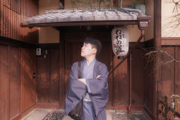
2026년 3월 28일 토요일. 교토에 왔습니다. 🇯🇵 인천공항 - 오사카 간사이 공항 경로였습니다. 탑승 전에 마티나 라운지에서 간단히 커피랑 아침 식사 했습니다. 오전 6시였음에도, 80%정도는 자리에 사람들이 있었고, 대부분 성인들이라 조용히 먹을 수 있었습니다. 해외여행...

korean
"얼마나 준비해놔야 하나요?" 재고 관리 (나의 경우, 제품의 라이센스 관리) 업무를 하다 보면 가장 자주 듣는 질문이다. 내가 있는 SW 분야는 라이센스가 있어야 유료 Program을 실행 할 수 있다. 이는 매우 비싸기 때문에 필요 수량만 보유하는 것이 효율적이다. 과제...

korean
Verilog(.v)와 SystemVerilog(.sv)는 반도체 설계에서 가장 널리 사용되는 HDL(Hardware Description Language) 파일입니다. RTL 설계부터 gate-level netlist까지, 설계 flow 전반에서 사용됩니다. 이 글에서는 두...

korean
VHDL과 EDIF는 Verilog만큼 자주 접하지는 않지만, 특정 분야와 legacy design에서 여전히 사용되는 중요한 format입니다. VHDL은 항공/군사 분야에서 선호되며, EDIF는 tool 간 netlist 교환에 사용됩니다. VHDL(.vhd)의 기본 구조...